Impedance circuit, power supply device

a technology of impedance circuit and power supply device, which is applied in the direction of logic circuit using specific components, logic circuits using semiconductor devices, pulse techniques, etc., can solve the problems of increasing the internal resistance of the battery, deteriorating performance, and the inability of sensing pair wires to always be connected near the load, so as to achieve the effect of negative impedance with eas

Inactive Publication Date: 2007-05-10
FUJITSU LTD
View PDF6 Cites 12 Cited by
  • Summary
  • Abstract
  • Description
  • Claims
  • Application Information

AI Technical Summary

Benefits of technology

[0016] The present invention has been made to solve problems described above, and has an object of providing an impedance circuit capable of realizing negative impedance with ease.
[0026] According to the present invention, negative impedance can be realized with ease. Further, the negative impedance can be used for compensation for a voltage drop.

Problems solved by technology

Furthermore, the sensing pair wire cannot always be connected near the load due to some reasons, such as mechanical interferences and physical limitations.
Another factor causing deterioration in performance is repetition of a temperature cycle.
Further, due to aging of the battery, the internal resistance of the battery increases and the voltage of the battery decreases at the time of outputting a large current.
This kind of power supply is expensive and has not yet been prevailing very much.

Method used


Image

  • Impedance circuit, power supply device
  • Impedance circuit, power supply device
  • Impedance circuit, power supply device

Examples


first embodiment

[First Embodiment]

[0036] In this embodiment, an impedance circuit using a current inverter circuit will be described.

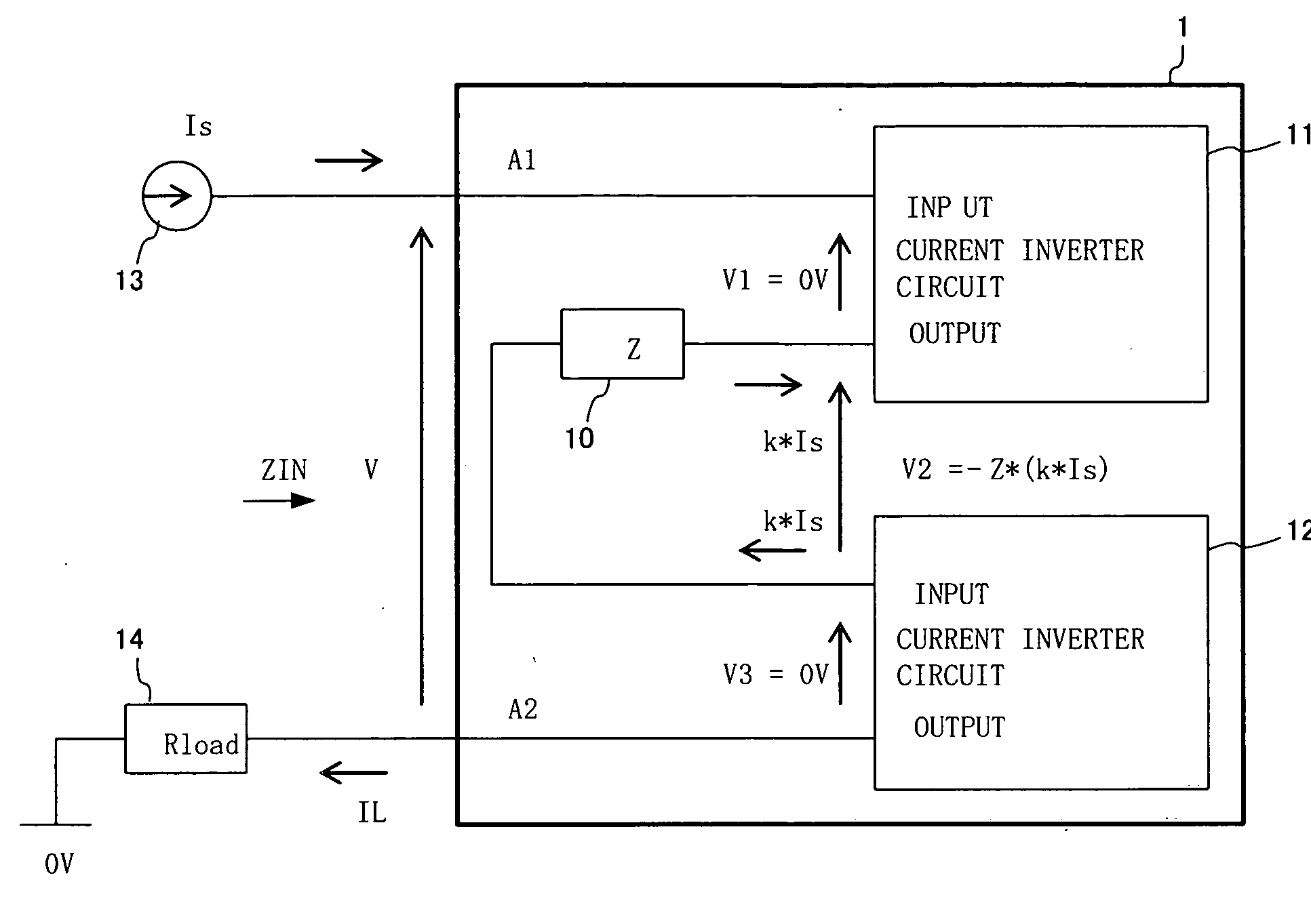
[0037] The structure of an impedance circuit according to the present invention will now be described first. FIG. 1 is a circuit diagram showing an example of the structure of the impedance circuit according to the present invention. This impedance circuit 1 has a passive circuit 10, and current inverter circuits 11 and 12. An input terminal of the impedance circuit 1 is denoted as A1, and an output terminal thereof is denoted as A2.

[0038] The input terminal of the current inverter circuit 11 is connected to an external current source 13 through A1. An output terminal of the current inverter circuit 11 is connected to an input terminal of the passive circuit 10. An input terminal of the current inverter circuit 12 is connected to an output terminal of the passive circuit 10. An output terminal of the current inverter circuit 12 is connected to an external load 14 th...

second embodiment

[Second Embodiment]

[0054] In the present embodiment, an impedance circuit using another current inverter circuit will be described.

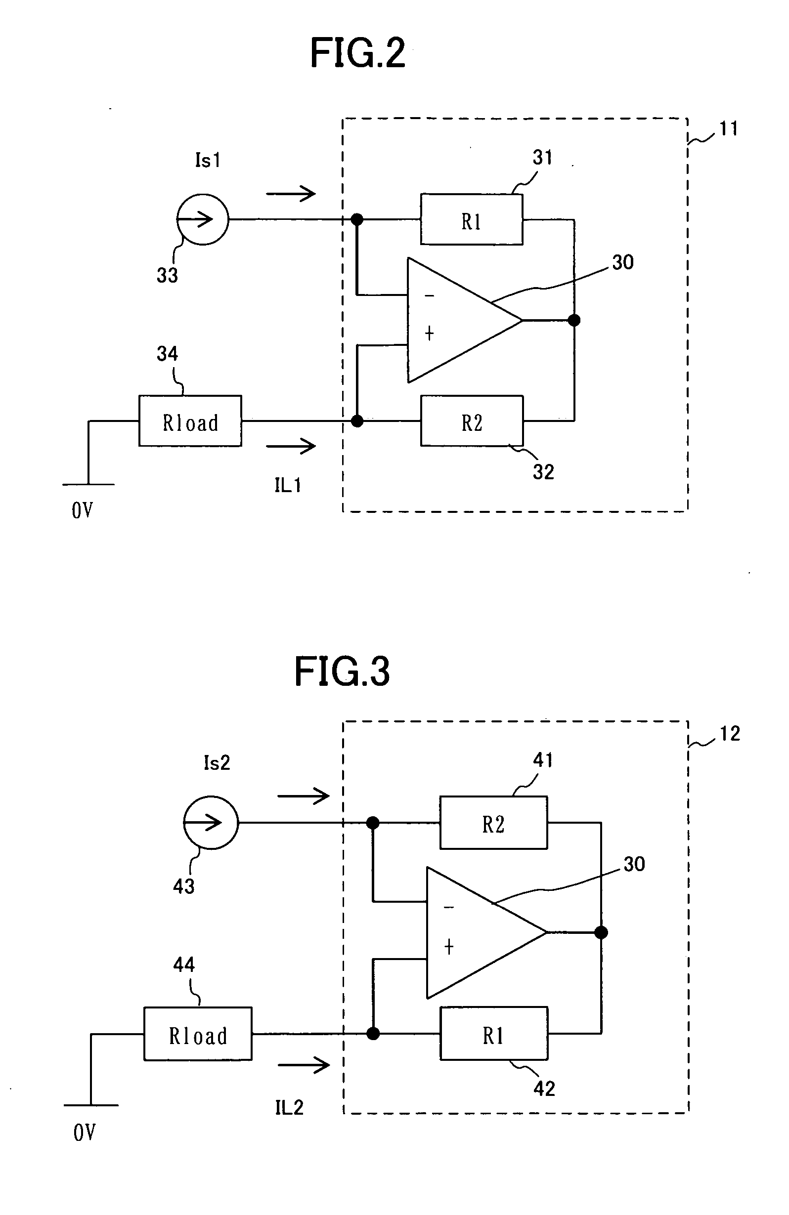
[0055]FIG. 4 is a circuit diagram showing another example of the structure of the impedance circuit according to the present invention. In FIG. 4, the same reference symbols as those of FIG. 1 denote identical or equivalent components to those shown in FIG. 1. Descriptions thereof will be omitted herefrom. Compared with FIG. 1, an impedance circuit 2 in place of the impedance circuit 1 is included in FIG. 3. Compared with the impedance circuit 1, the impedance circuit 2 has two current inverter circuits 13 in place of the current inverter circuits 11 and 12.

[0056] The current inverter circuits 13 will be described next.

[0057]FIG. 5 is a circuit diagram showing a third example of the structure of the current inverter circuit according to the present invention. In FIG. 5, the same reference symbols as those of FIG. 2 denote identical or equivalent compo...

third embodiment

[Third Embodiment]

[0061] In the present embodiment, a power supply device using an impedance circuit described above will be described.

[0062]FIG. 6 is a circuit diagram showing an example of the structure of a power supply device using the impedance circuit according to the present invention. In FIG. 6, the same reference symbols as those of FIG. 8 denote identical or equivalent components to those shown in FIG. 8. Descriptions thereof will be omitted herefrom. Compared with FIG. 8, FIG. 6 shows a resistor 113 in place of the resistor 103 as well as a resistor 114 in place of the resistor 104.

[0063] In this example, the resistor 114 is a resistance which a current path between a power supply section 101 and a load 102 has. The resistance value of the resistor 114 is expressed by RL1+RL2. At this time, an impedance circuit as described above is adopted as the resistor 113. The resistance value of the impedance circuit is set to a negative resistance −RL1−RL2. In this way, a voltage...


PUM


Abstract

There is disclosed an impedance circuit which realizes negative impedance with ease, and a power supply device having negative output impedance. An impedance circuit 1 connected to an external circuit comprises: a current inverter circuit 11 having an input terminal connected to outside; a passive circuit 10 having an input terminal connected to an output terminal of the current inverter circuit 11; and a current inverter circuit 12 having an input terminal connected to an output terminal of the passive circuit 10 and an output terminal connected to outside. The current inverter circuits 11 and 12 work in cooperation with each other, to make magnitude of impedance of the impedance circuit 1 proportional to impedance of the passive circuit 10, and to invert the polarity of the impedance of the impedance circuit 1.

Description

BACKGROUND OF THE INVENTION [0001] 1. Field of the Invention [0002] The present invention relates to an impedance circuit having negative impedance. [0003] 2. Description of the Related Art [0004] There have been demands for an impedance circuit having negative impedance. Particularly, a one-port circuit capable of varying resistance values from a negative resistance to a positive resistance. This one-port circuit cannot be a passive circuit constituted only by passive elements but has to be an active circuit including active elements such as transistors, FETs, and the like. [0005] An example where negative impedance is required Will now be described. [0006] In case of supplying electric power to a load from a direct current power supply, the potential difference between both ends of a load is requested to be maintained constant under a condition that the load current varies. If a direct current power supply having a remote sensing function is used in this case, the potential differ...

Claims


Application Information

Patent Timeline
Patent Type & Authority Applications(United States)
IPC IPC(8): H03K19/003
CPCH03H11/52H03H11/48
Inventor FUKUI, YUTAKA
Owner FUJITSU LTD
Why Eureka
Try Eureka