[0011]An
advantage of the present invention is that, at a point after shipment, it is possible to speedily carry out measurement of a display variation in an EL display apparatus and correction of the display variation.
[0012]According to one aspect of the present invention, there is provided an
electroluminescence display apparatus comprising a display section having a plurality of pixels arranged in a matrix, and a driving section which controls operation of the display section in accordance with a video
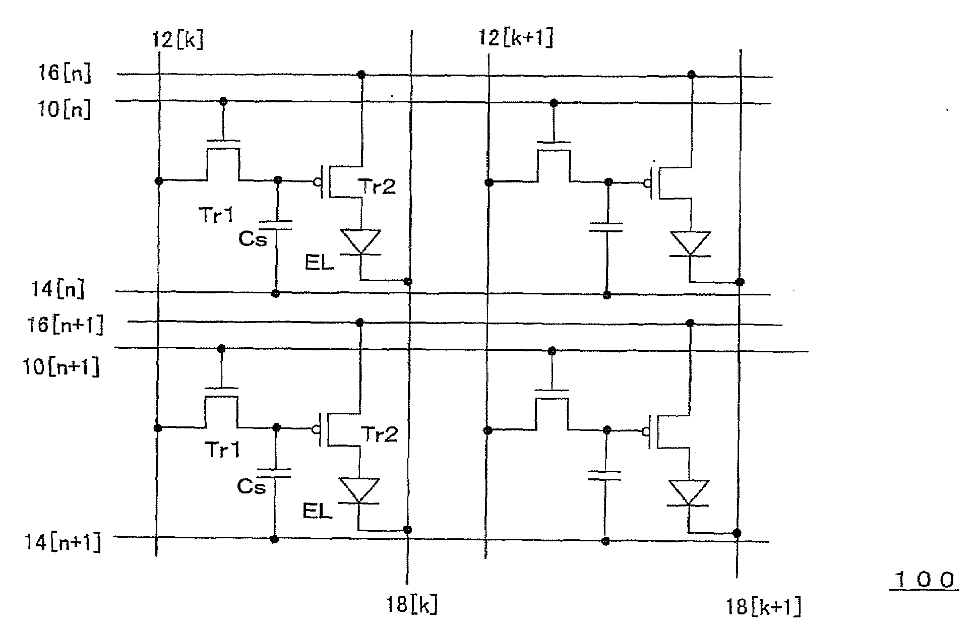
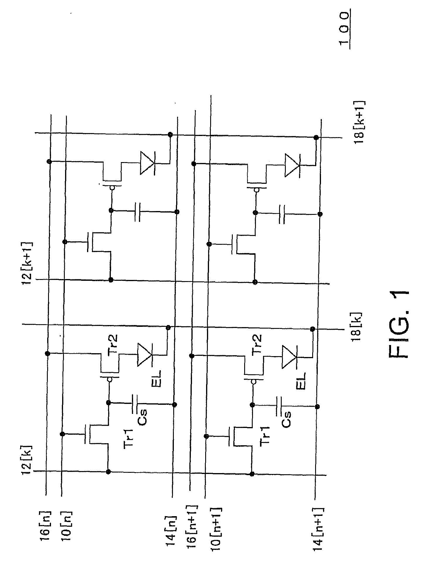
signal. The driving section comprises a driver which carries out row-direction drive and column-direction drive of the display section, a variation detecting section which detects an inspection result of a display variation in each pixel, and a correcting section which corrects the display variation. Each of the plurality of pixels in the display section comprises an
electroluminescence element, and an element driving
transistor which is connected to the electroluminescence element and controls a current that flows through the electroluminescence element. In the display section, a plurality of power supply lines for supplying power to electrodes of the electroluminescence elements in the respective pixels are provided along the column direction of the matrix. The variation detecting section comprises an inspection
signal generator which generates an inspection signal to be supplied to a pixel in a row to be inspected and supplies the inspection signal to the pixel in the inspected row, a current detection
amplifier which detects a current that flows through the electroluminescence element, and an analog-
digital converter which converts an analog current detection signal from the current detection
amplifier into a
digital signal. The current detection amplifier is configured to provide one current detection amplifier in correlation to multiple columns of the matrix, and each current detection amplifier is connected to the power supply lines. During a blanking period, a pixel in a predetermined inspected row is selected by the driver, and a current that flows through the electroluminescence element when an inspection ON signal which serves as the inspection signal and sets the electroluminescence element to an emission level is supplied to the selected pixel is detected by the current detection amplifier via the corresponding power supply line. The analog-
digital converter is configured to provide one successive approximation type analog-
digital converter in correlation to the multiple columns in a manner corresponding to the current detection amplifier. Each analog-digital converter comprises a
comparator which compares the analog current detection signal from the current detection amplifier with a reference signal, a successive approximation register which successively changes a
data value from higher-order bit side taking into account a comparison signal from the
comparator and supplies the changed value to a digital-analog converter, and a digital-analog converting section which converts a
digital signal from the successive approximation register into an
analog signal and supplies the converted
analog signal as the reference signal to the
comparator. The digital-analog converting section is commonly shared by a plurality of the analog-digital
converters.
[0013]According to another aspect of the present invention, in the above-described apparatus, during the blanking period, the inspection
signal generator supplies to the pixel in the inspected row, as the inspection signal, the inspection ON signal and an inspection OFF signal that sets the electroluminescence element to a non-emission level. The current detection amplifier detects an ON current that flows through the electroluminescence element when the inspection ON signal obtained from the power supply line is applied, and an OFF current obtained when the inspection OFF signal is applied. The analog-digital converter converts an output from the current detection amplifier into corresponding digital ON current detection signal and digital OFF current detection signal. A
subtractor calculates a difference between the digital ON current detection signal and the digital OFF current detection signal. The correcting section performs correction using a current difference signal in accordance with the calculated current difference between the digital ON current detection signal and the digital OFF current detection signal.
[0014]According to another aspect of the present invention, in the above-described apparatuses, the driver comprises a digital-analog display data converter which converts a
data signal that is in accordance with a display content and is processed as a
digital signal into an analog
data signal to be supplied to each pixel in the display section. A
resistor string of the digital-analog converting section of the successive approximation type analog-digital
converters is commonly shared as a
resistor string of the digital-analog display data converter.
[0015]According to another aspect of the present invention, in the above-described apparatuses, each of the plurality of pixels further comprises a storage
capacitor which retains a gate potential of the element driving
transistor. A first
electrode of the storage
capacitor is connected to a gate of the element driving transistor, and a second
electrode of the storage
capacitor is connected to a capacitor line provided for each row. The driving section includes a capacitor line controller. The capacitor line controller functions to, during an inspection signal writing period within the blanking period, set a potential of the capacitor line of the inspected row to a first potential that sets the gate potential of the element driving transistor to a non-operation level, and, during a
data signal rewriting period until end of the blanking period, set the potential of the capacitor line of the inspected row to a second potential that places the element driving transistor in an operable state.
[0016]According to another aspect of the present invention, in the above-described apparatuses, the capacitor line controller further functions to, during the blanking period, fix potentials of all the capacitor lines in the display section other than the capacitor line for the inspected row to the first potential.

