Electroluminescence display apparatus

a display apparatus and electroluminescent technology, applied in static indicating devices, instruments, material analysis, etc., can solve the problems of unfavorable correction of display variations, unfavorable adjustment of display variations, and reduced yield, so as to speedily carry out measurement of display variations

Active Publication Date: 2011-08-30
SEMICON COMPONENTS IND LLC
View PDF4 Cites 7 Cited by
  • Summary
  • Abstract
  • Description
  • Claims
  • Application Information

AI Technical Summary

Benefits of technology

[0011]An advantage of the present invention is that, at a point after shipment, it is possible to speedily carry out measurement of a display variation in an EL display apparatus and correction of the display variation.
[0012]According to one aspect of the present invention, there is provided an electroluminescence display apparatus comprising a display section having a plurality of pixels arranged in a matrix, and a driving section which controls operation of the display section in accordance with a video signal. The driving section comprises a driver which carries out row-direction drive and column-direction drive of the display section, a variation detecting section which detects an inspection result of a display variation in each pixel, and a correcting section which corrects the display variation. Each of the plurality of pixels in the display section comprises an electroluminescence element, and an element driving transistor which is connected to the electroluminescence element and controls a current that flows through the electroluminescence element. In the display section, a plurality of power supply lines for supplying power to electrodes of the electroluminescence elements in the respective pixels are provided along the column direction of the matrix. The variation detecting section comprises an inspection signal generator which generates an inspection signal to be supplied to a pixel in a row to be inspected and supplies the inspection signal to the pixel in the inspected row, a current detection amplifier which detects a current that flows through the electroluminescence element, and an analog-digital converter which converts an analog current detection signal from the current detection amplifier into a digital signal. The current detection amplifier is configured to provide one current detection amplifier in correlation to multiple columns of the matrix, and each current detection amplifier is connected to the power supply lines. During a blanking period, a pixel in a predetermined inspected row is selected by the driver, and a current that flows through the electroluminescence element when an inspection ON signal which serves as the inspection signal and sets the electroluminescence element to an emission level is supplied to the selected pixel is detected by the current detection amplifier via the corresponding power supply line. The analog-digital converter is configured to provide one successive approximation type analog-digital converter in correlation to the multiple columns in a manner corresponding to the current detection amplifier. Each analog-digital converter comprises a comparator which compares the analog current detection signal from the current detection amplifier with a reference signal, a successive approximation register which successively changes a data value from higher-order bit side taking into account a comparison signal from the comparator and supplies the changed value to a digital-analog converter, and a digital-analog converting section which converts a digital signal from the successive approximation register into an analog signal and supplies the converted analog signal as the reference signal to the comparator. The digital-analog converting section is commonly shared by a plurality of the analog-digital converters.
[0013]According to another aspect of the present invention, in the above-described apparatus, during the blanking period, the inspection signal generator supplies to the pixel in the inspected row, as the inspection signal, the inspection ON signal and an inspection OFF signal that sets the electroluminescence element to a non-emission level. The current detection amplifier detects an ON current that flows through the electroluminescence element when the inspection ON signal obtained from the power supply line is applied, and an OFF current obtained when the inspection OFF signal is applied. The analog-digital converter converts an output from the current detection amplifier into corresponding digital ON current detection signal and digital OFF current detection signal. A subtractor calculates a difference between the digital ON current detection signal and the digital OFF current detection signal. The correcting section performs correction using a current difference signal in accordance with the calculated current difference between the digital ON current detection signal and the digital OFF current detection signal.
[0014]According to another aspect of the present invention, in the above-described apparatuses, the driver comprises a digital-analog display data converter which converts a data signal that is in accordance with a display content and is processed as a digital signal into an analog data signal to be supplied to each pixel in the display section. A resistor string of the digital-analog converting section of the successive approximation type analog-digital converters is commonly shared as a resistor string of the digital-analog display data converter.
[0015]According to another aspect of the present invention, in the above-described apparatuses, each of the plurality of pixels further comprises a storage capacitor which retains a gate potential of the element driving transistor. A first electrode of the storage capacitor is connected to a gate of the element driving transistor, and a second electrode of the storage capacitor is connected to a capacitor line provided for each row. The driving section includes a capacitor line controller. The capacitor line controller functions to, during an inspection signal writing period within the blanking period, set a potential of the capacitor line of the inspected row to a first potential that sets the gate potential of the element driving transistor to a non-operation level, and, during a data signal rewriting period until end of the blanking period, set the potential of the capacitor line of the inspected row to a second potential that places the element driving transistor in an operable state.
[0016]According to another aspect of the present invention, in the above-described apparatuses, the capacitor line controller further functions to, during the blanking period, fix potentials of all the capacitor lines in the display section other than the capacitor line for the inspected row to the first potential.

Problems solved by technology

In a current active matrix EL display apparatus having a TFT in each pixel, a brightness unevenness occurs among the EL elements because of display unevenness caused by the TFT, in particular, a variation in the threshold value Vth of the TFT, which is a major cause of reduction in yield.
The method of measuring the brightness variation by causing the EL panel to emit light and capturing an image of the emission with a camera as described in Reference Document 1 cannot be conducted after shipment, such that this method does not enable execution of corrections with respect to changes of the panel over time or the like.

Method used


Image

  • Electroluminescence display apparatus
  • Electroluminescence display apparatus
  • Electroluminescence display apparatus

Examples


Embodiment Construction

[0033]A preferred embodiment of the present invention (hereinafter referred to as “embodiment”) will now be described with reference to the drawings.

[Detection Principle]

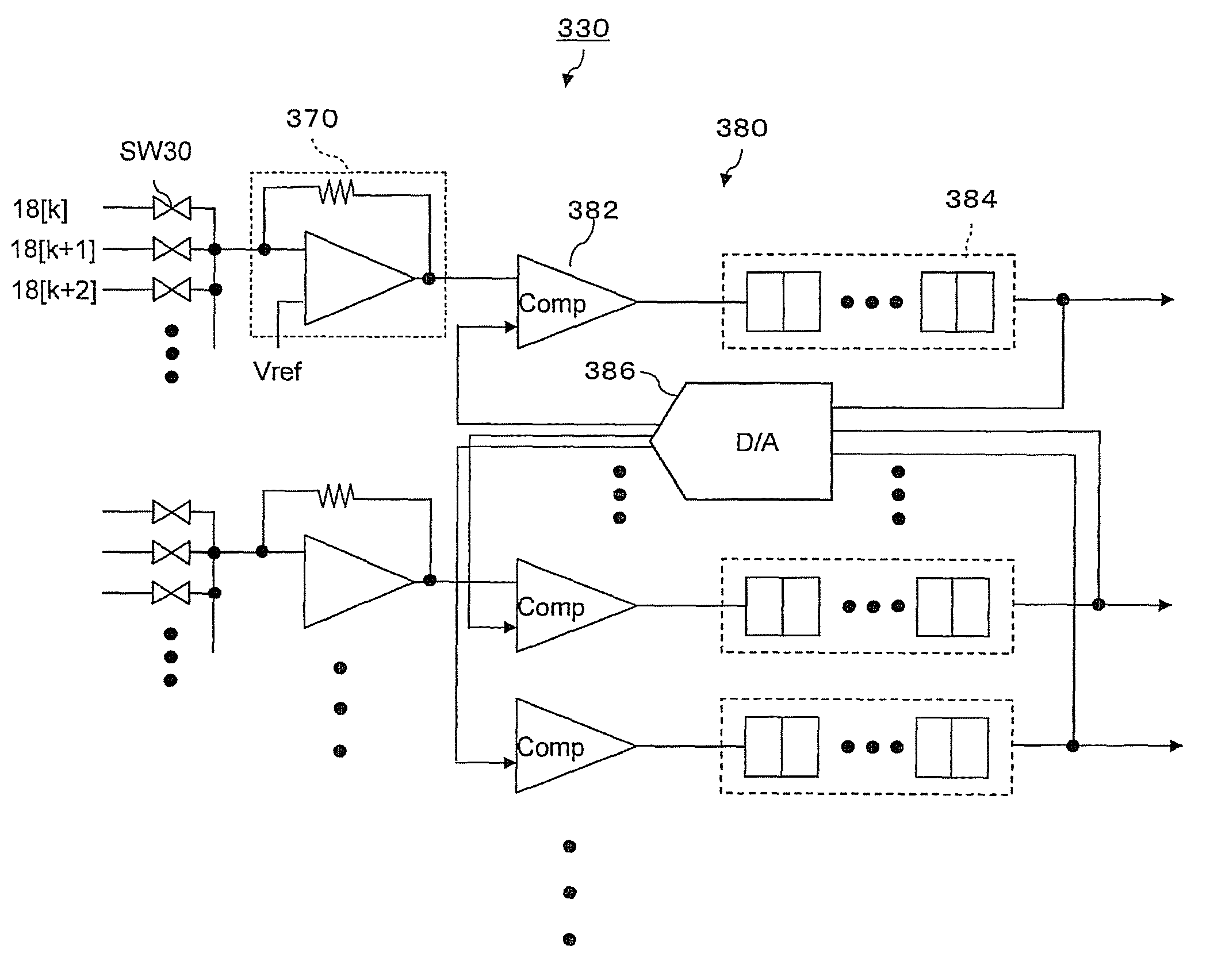
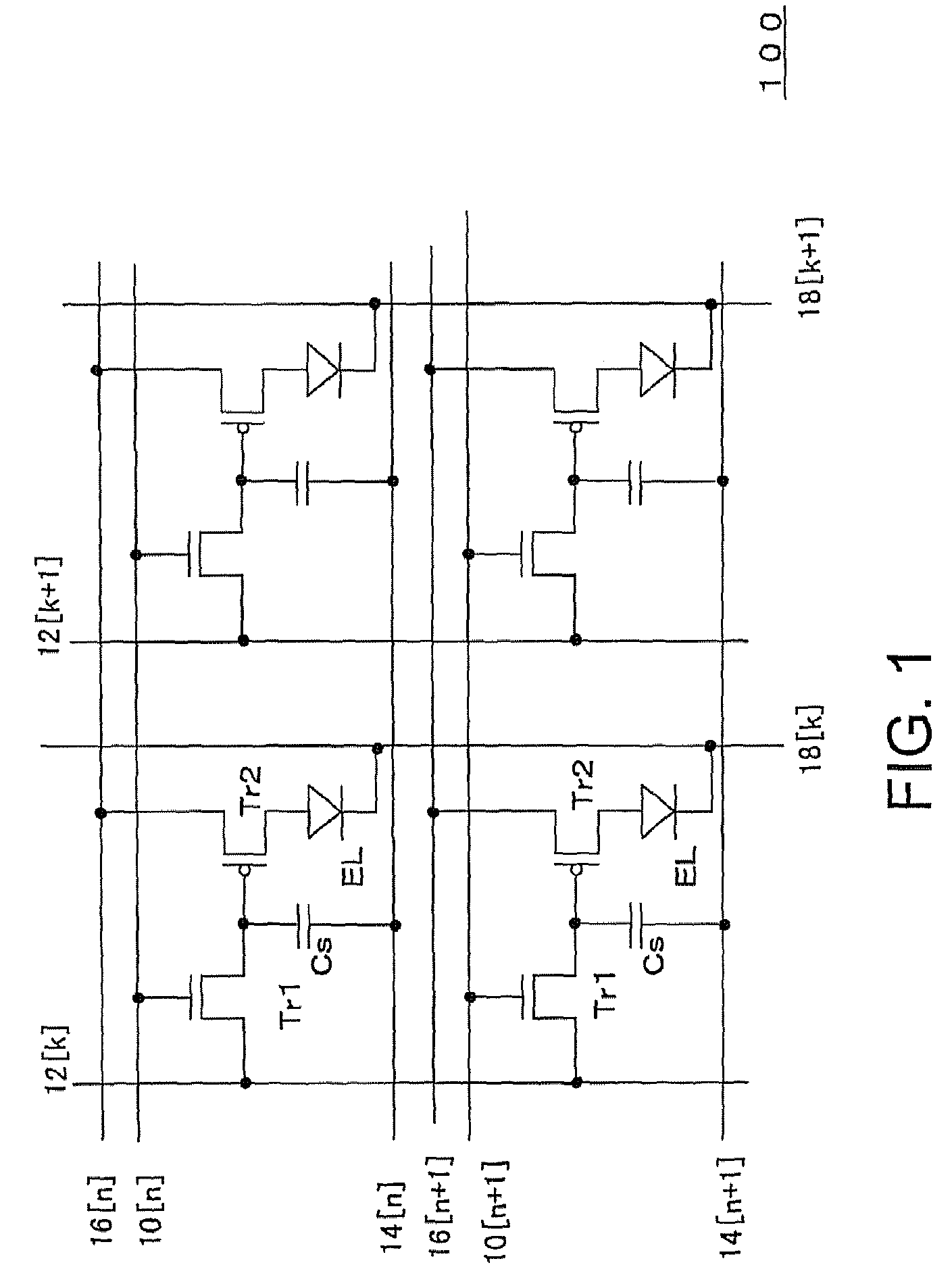
[0034]In the embodiment, a display apparatus is an active matrix organic electroluminescence (EL) display apparatus, and a display section having a plurality of pixels is formed on an EL panel 100. FIG. 1 is a diagram showing an example equivalent circuit structure of an active matrix EL display apparatus according to the embodiment. A plurality of pixels are arranged in the display section of the EL panel 100 in a matrix form. Formed along a horizontal (H) scan direction (row direction) of the matrix are a selection line (gate line GL) 10 on which a selection signal is sequentially output, and a power supply line 16 (VL) for supplying a drive power supply PVDD to an organic EL element 18 (hereinafter simply referred to as “EL element”) which is an element to be driven. A data line 12 (DL) on which a data signal (Vs...


PUM


Abstract

During a blanking period of a video signal, an element driving transistor for controlling a drive current supplied to an EL element is operated in its saturation region to thereby set the EL element to an emission level, and a current flowing through the EL element at that time is detected. Each current detector includes a current detection amplifier and a successive approximation type AD converter, and a DA converter of the successive approximation type AD converter is commonly shared among a plurality of the AD converters. With this arrangement, sufficient AD converting speed can be attained while using a simple structure to execute current detection for correcting display variations.

Description

CROSS-REFERENCE TO RELATED APPLICATIONS[0001]The entire disclosure of Japanese Patent Application No. 2007-092616 including specification, claims, drawings, and abstract is incorporated herein by reference.BACKGROUND OF THE INVENTION[0002]1. Field of the Invention[0003]The present invention relates to a display apparatus having an electroluminescence element in each pixel, and particularly to such a display apparatus having a function of correcting a display variation.[0004]2. Description of the Related Art[0005]Electroluminescence (hereinafter referred to as “EL”) display apparatuses in which an EL element which is a self-emissive element is employed as a display element in each pixel are expected as a flat display apparatus of the next generation, and are being researched and developed.[0006]After an EL panel is created in which an EL element and a thin film transistor (hereinafter referred to as “TFT”) or the like for driving the EL element for each pixel are formed on a substrat...

Claims


Application Information

Patent Timeline
Patent Type & Authority Patents(United States)
IPC IPC(8): G09G3/30H05B44/00
CPCG09G3/3233G09G3/3291G09G2310/0297G09G2320/0233G09G2320/0285G09G2320/0295
Inventor MATSUO, YUICHIOGAWA, TAKASHI
Owner SEMICON COMPONENTS IND LLC
Why Eureka
Try Eureka