

Printed Circuit Board and Its Designing Method, and Designing Method of Ic Package Terminal and Its Connecting Method
a printing circuit board and design method technology, applied in the direction of resist details, electrical apparatus construction details, instruments, etc., can solve the problems of insufficient electric insulation, difficult to develop inexpensive printed circuit boards applicable to such narrow pitches, and difficulty in drawing out the wiring pattern connected to the soldering land. the effect of cost reduction
- Summary
- Abstract
- Description
- Claims
- Application Information
AI Technical Summary
Benefits of technology
Problems solved by technology
Method used
Image

Examples
embodiment 1
Preferred Embodiment 1
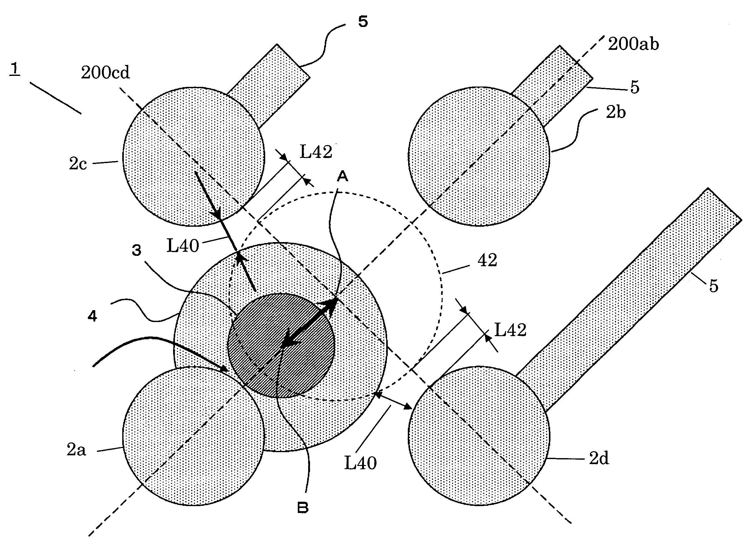
[0074]FIG. 1 shows configuration of soldering lands and through-hole upper lands in preferred embodiment 1 of the invention.
[0075]In FIG. 1, on a principal surface of a printed circuit board 1, soldering lands 2a, 2b, 2c, and 2d are formed for connecting terminals of BGA through solder balls. These four soldering lands are arrayed in lattice. Also on the principal surface of the printed circuit board 1, wiring patterns 5 are provided for drawing out the wiring from through-holes 3, through-hole upper lands 4 provided on the through-holes 3, and soldering lands 2b, 2c, 2d, in the outward direction through the principal surface 1a of the printed circuit board 1. The through-hole 3 is surrounded by soldering lands 2a to 2d. In FIG. 1, the number of soldering lands 2a of same potential connected to the through-hole upper land 4 is one. As a matter of course, the number of soldering lands of same potential as through-hole 3 is not limited to one. Two or three solder...
other example 1
of Preferred Embodiment 1
[0095]FIG. 4 is a diagram showing other form of printed circuit board in preferred embodiment 1. Four soldering lands 2a2, 2b2, 2c2, and 2d2 are disposed in lattice. FIG. 4 shows two soldering lands 2a2, 2d2 of same potential as through-hole upper land 4. The soldering lands 2b2, 2c2, and the soldering lands 2a2, 2d2 are different in potential, that is, they are formed as soldering of different potential. Diagonal line 400ab links centers of soldering lands 2a2 and 2b2. Diagonal line 400cd links centers of soldering lands 2c2 and 2d2. The crossing point of diagonal line 400ab and diagonal line 400cd is shown as intersection A40. The central point B30 of through-hole 3 is eccentric by specified extent in vertical downward direction from intersection A40 in front view of FIG. 4. In FIG. 4, the reason of being eccentric in vertical downward direction is that the soldering lands 2a2 and 2d2 of same potential as through-hole 3 are present in this direction. That ...
other example 2
of Preferred Embodiment 1
[0102]FIG. 6 is a diagram showing a other example 2 of preferred embodiment 1. In FIG. 6, three soldering lands are of same potential as through-hole upper land 4, and the remaining one is of different potential. Diagonal line 800ab links the central points of soldering lands 2a4 and 2b4. Diagonal line 800cd links the central points of soldering lands 2c4 and 2d4. In this case, the area 600 specified by formula 1 and formula 2 is as shown in FIG. 6. That is, the position of through-hole 3 is determined so that the central point of through-hole 3 may be present in the area 600.
[0103]In FIG. 6, the area satisfying the conditions of formula 1 and formula 2 is indicated as area 600. The area 600 is enclosed by six line segments. First line segment 602 is a circle concentric with soldering land 2c4, and part of circle of which radius is (rS+rT). Second line segment 604 is a straight line linking the central points of soldering lands 2c4 and 2a4. Third line segmen...
PUM
| Property | Measurement | Unit |
|---|---|---|
| Thickness | aaaaa | aaaaa |
| Diameter | aaaaa | aaaaa |
| Radius | aaaaa | aaaaa |
Abstract
Description
Claims
Application Information