Liquid crystal display device

a technology of liquid crystal display and display device, which is applied in the direction of semiconductor devices, instruments, optics, etc., can solve the problems of difficult to raise the aperture ratio, reduce the area per pixel that can be used to form the electrodes of storage capacitors, and non-transparent metal

Active Publication Date: 2009-03-05
PANASONIC LIQUID CRYSTAL DISPLAY CO LTD +1
View PDF10 Cites 136 Cited by
  • Summary
  • Abstract
  • Description
  • Claims
  • Application Information

AI Technical Summary

Benefits of technology

[0069]An effect obtained from the representative embodiments of the pr

Problems solved by technology

When one of the electrodes that constitute the storage capacitor is metal as in the above-mentioned structures (2) to (4), the non-transparent metal part makes it difficult to raise the aperture ratio, particularly in the case of a transmissive liquid crystal display device.
However, reducing the pixel dimensions for the purpose of obtaining an ultra-high definition liquid crystal display panel, such as one for portable terminal that have a VGA-level resolution, accordingly reduces the area per pixel that

Method used


Image

  • Liquid crystal display device
  • Liquid crystal display device
  • Liquid crystal display device

Examples


first embodiment

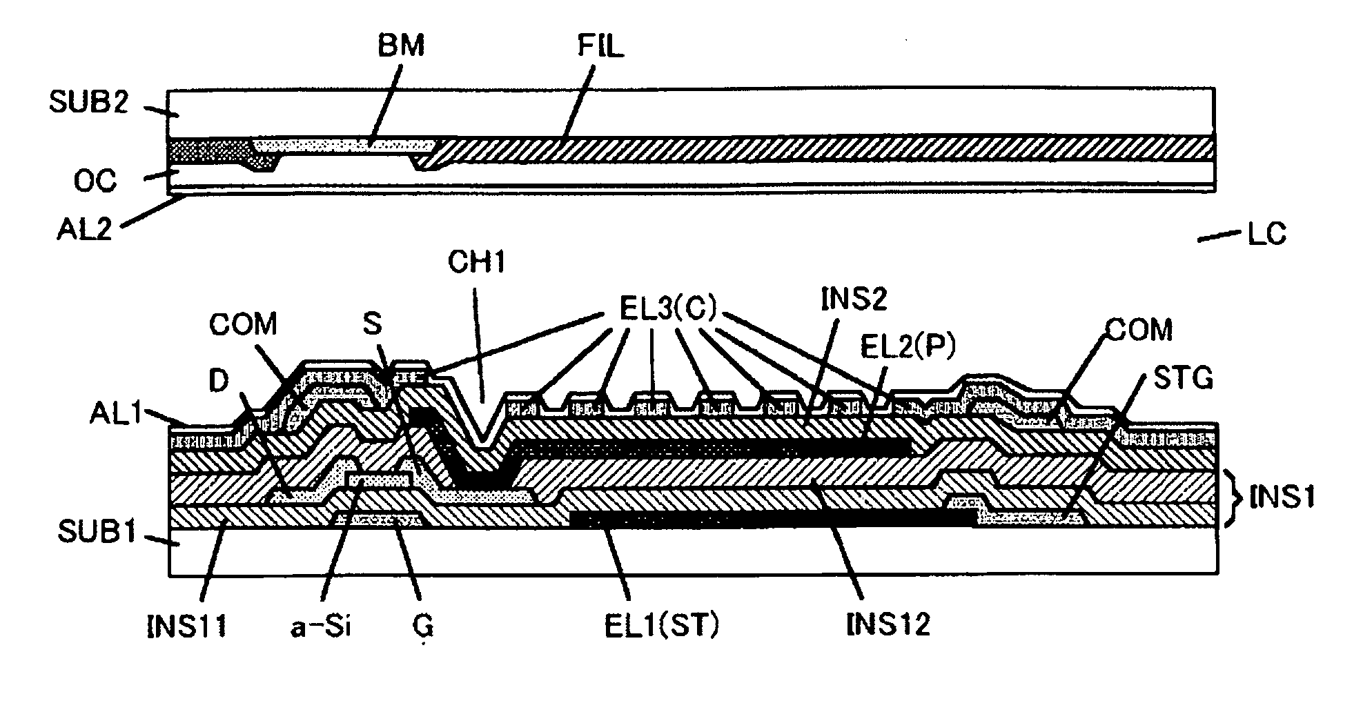
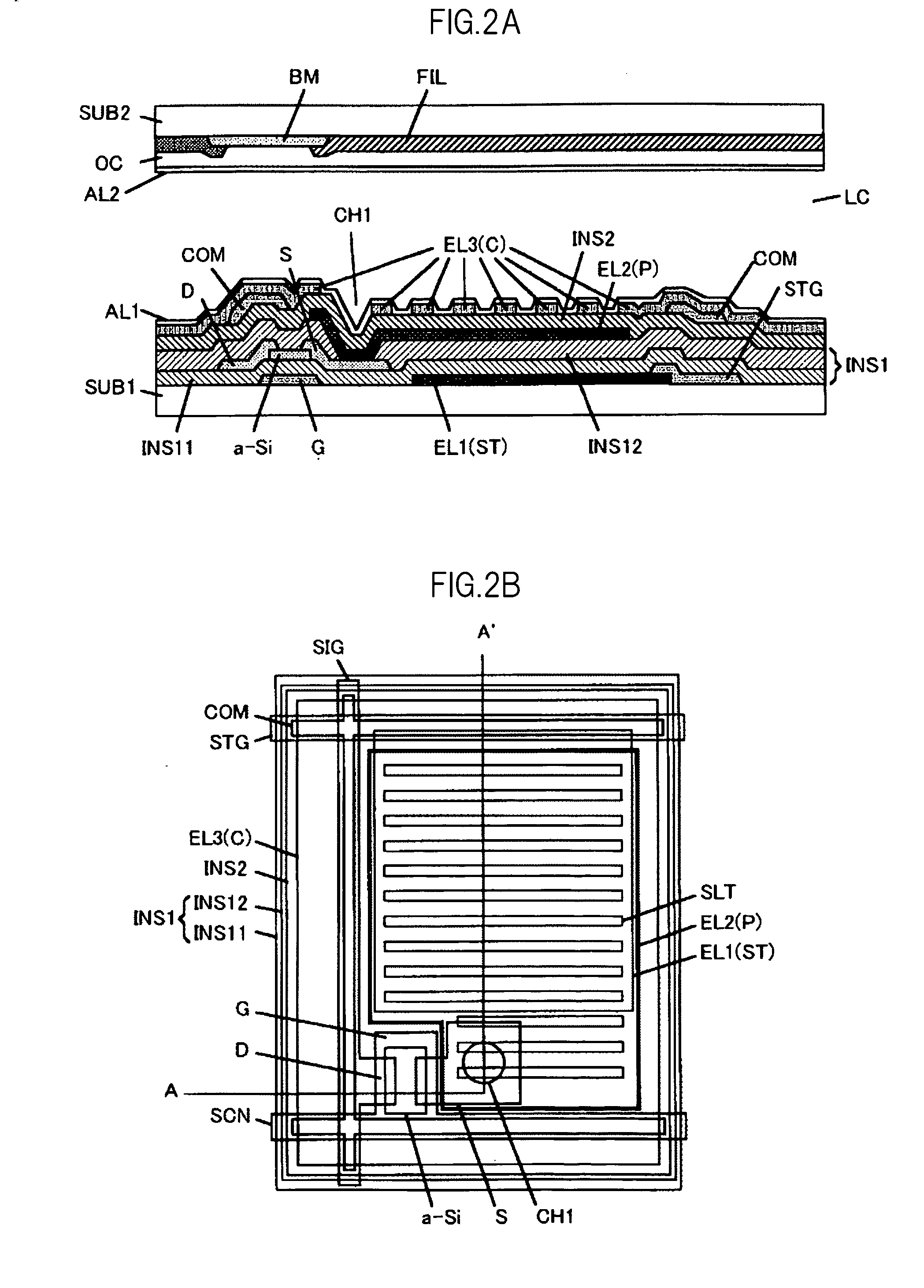
[0121]A first embodiment of the present invention, as well as second to sixth embodiments of the present invention which will be described later, deals with an IPS liquid crystal display device in which the second transparent electrode EL2 serves as a pixel electrode, whereas the first transparent electrode EL1 and the third transparent electrode EL3 serve as a storage capacitor electrode and as a counter electrode, respectively.

[0122]FIGS. 2A and 2B are schematic diagrams showing a pixel structure in the liquid crystal display device according to the first embodiment of the present invention. FIG. 2A shows the sectional structure of a pixel and FIG. 2B shows the plan view structure of the pixel on the TFT substrate side. The sectional structure shown in FIG. 2A corresponds to a view taken along the line A-A′ shown in FIG. 2B.

[0123]On the first substrate SUB1, scanning lines SCN and as many storage capacitor wiring lines STG are provided so that the former and the latter are associa...

second embodiment

[0161]FIGS. 6A and 6B are schematic diagrams showing a pixel structure in a liquid crystal display device according to the second embodiment of the present invention. Shown in FIG. 6A is the sectional structure of a pixel, and shown in FIG. 6B is the plan view structure of the pixel on the TFT substrate side. The sectional structure of FIG. 6A corresponds to a view taken along the line A-A′ shown in FIG. 6B.

[0162]The difference from the first embodiment is that, instead of using the common electrode wiring line COM between the transparent counter electrode EL3 (C) and the second insulating film INS2, the second embodiment makes the storage capacitor wiring line STG formed in the gate layer double as the common electrode wiring line COM.

[0163]The transparent counter electrode EL3 (C) in the second embodiment is reduced in resistance as in the first embodiment by forming openings (contact holes CH2 to CH4) in a portion of the gate insulating film INS11, a portion of the passivation fi...

third embodiment

[0179]FIGS. 9A and 9B are schematic diagrams showing a pixel structure in a liquid crystal display device according to the third embodiment of the present invention. Shown in FIG. 9A is the sectional structure of a pixel, and shown in FIG. 9B is the plan view structure of the pixel on the TFT substrate side. The sectional structure of FIG. 9A corresponds to a view taken along the line A-A′ shown in FIG. 9B.

[0180]The difference from the first embodiment is that the third embodiment uses the passivation film INS12 as the second insulating film INS2 by moving the transparent pixel electrode EL2 (P) to a place between the gate insulating film INS11 and the passivation film INS12 and constituting the first insulating film INS1 solely from the gate insulating film INS11.

[0181]Accordingly, this embodiment can reduce one insulating film and, in addition, can easily form a sufficiently large storage capacitor in a pixel having reduced pixel dimensions because the capacitance per unit area of...


PUM


Abstract

To form a sufficiently large storage capacitor, a liquid crystal display device includes a liquid crystal display panel having a first substrate, a second substrate, and a liquid crystal held between the first substrate and the second substrate, the liquid crystal display panel having multiple pixels arranged in matrix. The first substrate has, in a transmissive display area provided in each of the pixels, a laminated structure containing a first transparent electrode, a first insulating film, a second transparent electrode, a second insulating film, and a third transparent electrode which are laminated in this order. The first transparent electrode and the second transparent electrode are electrically insulated from each other and together form a first storage capacitor through the first insulating film, and the second transparent electrode and the third transparent electrode are electrically insulated from each other and together form a second storage capacitor through the second insulating film.

Description

CROSS-REFERENCE TO RELATED APPLICATION[0001]The present application claims priority from Japanese application JP 2007-228412 filed on Sep. 4, 2007, the content of which is hereby incorporated by reference into this application.BACKGROUND OF THE INVENTION[0002]1. Field of the Invention[0003]The present invention relates to a liquid crystal display device, and more particularly, to a technology effectively applied to a liquid crystal display device that has a liquid crystal display panel with fine pixel dimensions.[0004]2. Description of the Related Art[0005]A liquid crystal display device is composed of a pair of substrates (for example, glass substrates) and a liquid crystal composition sealed in a gap between the substrates. Specifically, in the case of an in-plane switching (IPS) liquid crystal display device, for example, thin film transistors with amorphous silicon or other semiconductor layers, pixel electrodes, signal lines, scanning lines, gate electrodes, counter electrodes,...

Claims


Application Information

Patent Timeline
IPC IPC(8): G02F1/1335G02F1/1343
CPCG02F1/134363G02F1/136213H01L27/12H01L27/1214H01L27/13G02F1/136286G02F2001/13629H01L27/1255G02F1/136227G02F1/13439G02F1/133345G02F2001/13606G02F1/1368H01L27/124G02F1/13629G02F1/133512G02F1/133514
Inventor SASAKI, TOHRUOCHIAI, TAKAHIRO
Owner PANASONIC LIQUID CRYSTAL DISPLAY CO LTD
Why Eureka
Try Eureka