
Substrate treatment apparatus
a substrate treatment and substrate technology, applied in the direction of electrical equipment, thin material processing, article separation, etc., can solve the problems of increasing the occupied floor area of the coating/developing apparatus, the cassette cannot be loaded on the cassette loading table, etc., to achieve the effect of not without increasing the occupied floor area, and without lowering the throughput of the substrate treatment apparatus
- Summary
- Abstract
- Description
- Claims
- Application Information
AI Technical Summary
Benefits of technology
Problems solved by technology
Method used
Image

Examples
Embodiment Construction
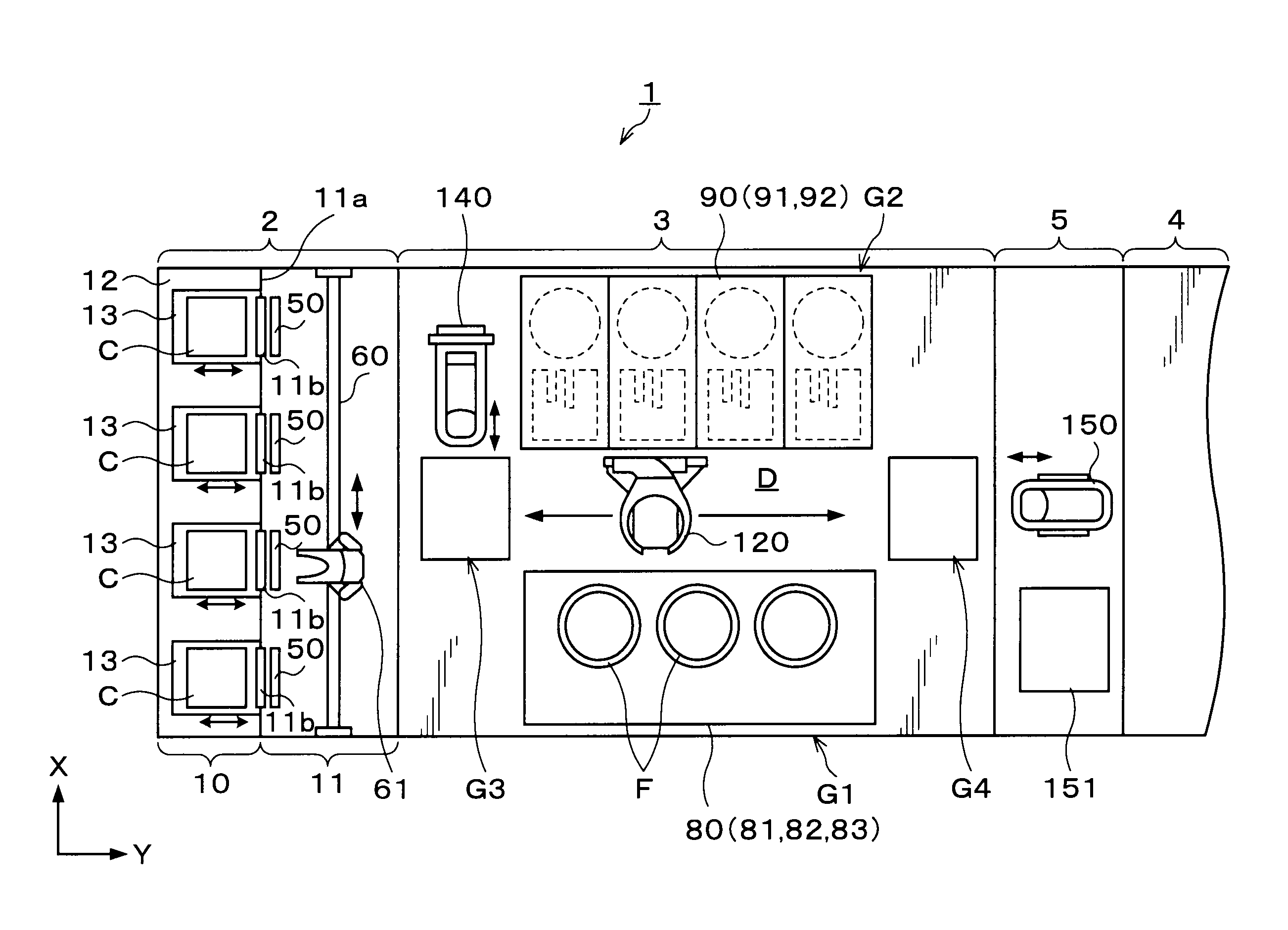
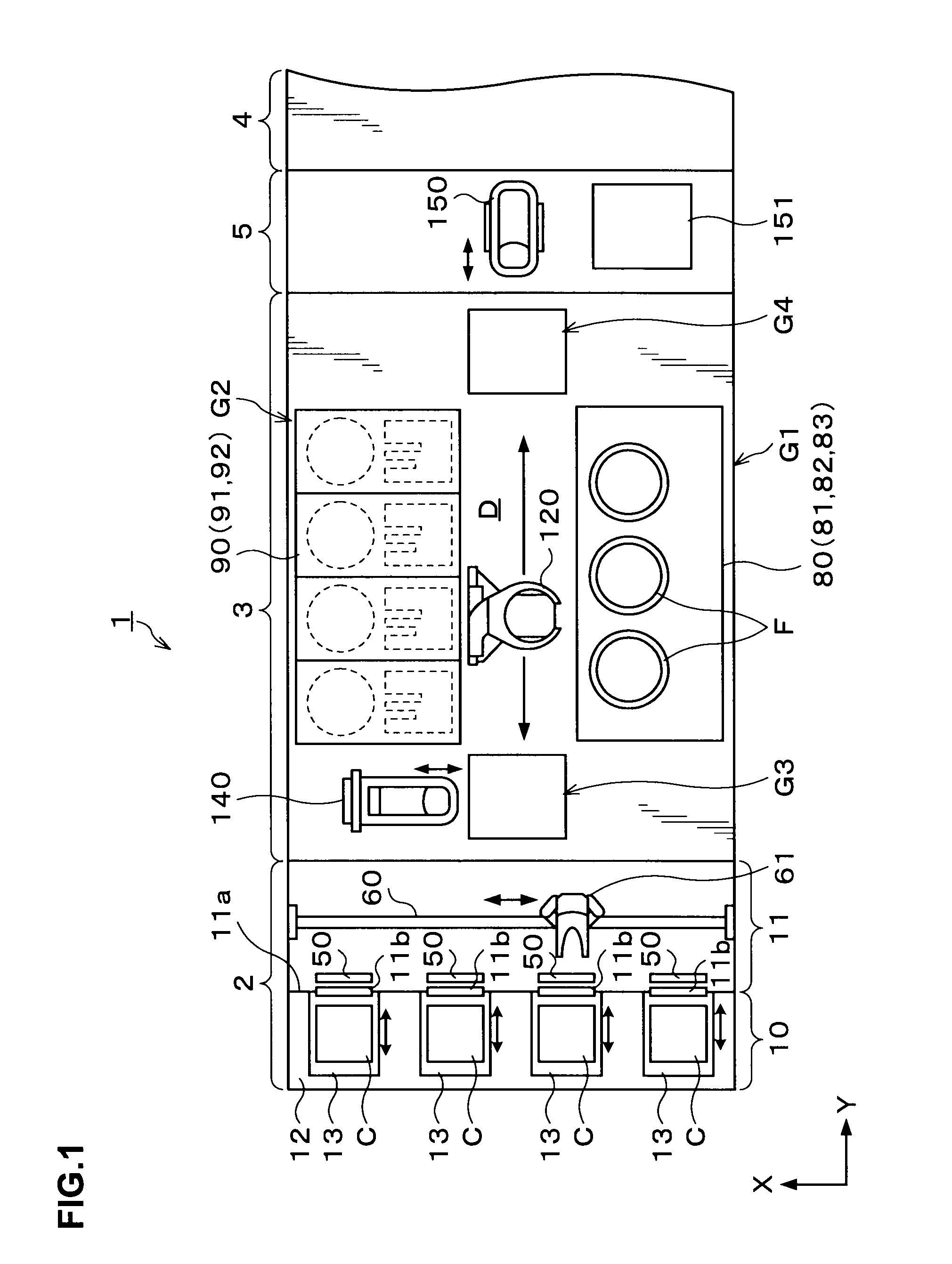
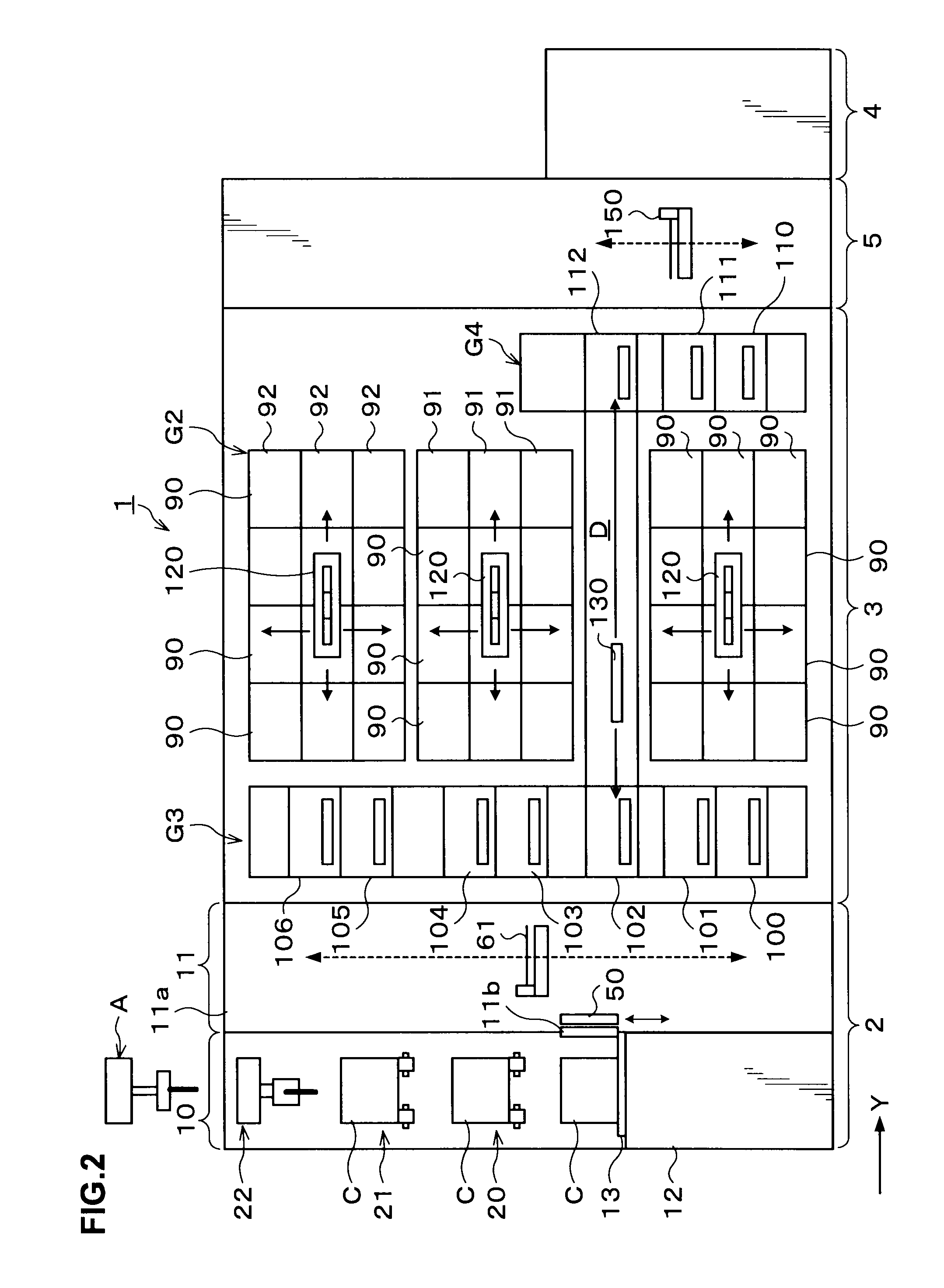
[0041]Hereinafter, embodiments of the present invention will be described. FIG. 1 is an explanatory view schematically showing an inner structure of a coating / developing apparatus 1 as a substrate treatment apparatus according to the present invention. FIGS. 2 and 3 are side views each schematically showing the inner structure of the coating / developing apparatus 1.
[0042]As shown in FIG. 1, the coating / developing apparatus 1 has a structure in which a cassette station 2, a treatment station 3, and an interface station 5 are integrally connected to each other. A cassette C is carried to / from the cassette station 2 from / to outside. The treatment station 3 serves as a substrate treatment portion including a plurality of various kinds of treatment units that perform predetermined treatments in a sheet-feed manner in a photolithography. Through the interface station 5 adjacent to the treatment station 3, a wafer W is carried to / received from an exposing apparatus 4.
[0043]The cassette stat...
PUM
 Abstract
Description
Claims
Application Information