Pixel and organic light emitting display

a technology of organic light and display, applied in the field of pixels and organic light emitting displays, can solve the problem that images with desired brightness may not be displayed

Inactive Publication Date: 2009-06-11
SAMSUNG DISPLAY CO LTD
View PDF6 Cites 27 Cited by
  • Summary
  • Abstract
  • Description
  • Claims
  • Application Information

AI Technical Summary

Benefits of technology

[0015]In order to achieve the foregoing and / or other aspects of the present invention, according to a first aspect of an exemplary embodiment of the present invention, there is provided a pixel positioned at an ith pixel row, the pixel including an organic light emitting diode (OLED), a pixel circuit including a driving transistor for supplying a current to the OLED, the pixel circuit being configured to compensate for a threshold voltage variation of the driving transistor, the pixel circuit further including a storage capacitor coupled between a gate electrode of the driving transistor and an (i−1)th emission control line, and a compensating unit for controlling a voltage of the gate electrode of the driving transistor to compensate for deterioration of the OLED. The compensating unit includes a first compensating unit transistor and a second compensating unit transistor coupled between the OLED and a first power source, a first feedback capacitor and a second feedback capacitor positioned between a second node between the first compensating unit transistor and the second compensating unit transistor and a first node between the gate electrode of the driving transistor and the storage capacitor, and a third compensating unit transistor coupled between a third node between the first feedback capacitor and the second feedback capacitor and a reference voltage source.
[0016]According to a second aspect of an exemplary embodiment of the present invention, there is provided an organic light emitting display including: a scan driver for supplying scan signals to scan lines and for supplying emission control signals to emission control lines; a data driver for supplying data signals to data lines; and pixels positioned at regions defined by the scan lines and the data lines, wherein a pixel positioned at an ith pixel row among the pixels includes: an organic light emitting diode (OLED); a pixel circuit including a driving transistor for supplying a current to the OLED and for compensating for a threshold voltage variation of the driving transistor, the pixel circuit further including a storage capacitor coupled between a gate electrode of the driving transistor and an (i−1)th emission control line; and a compensating unit for controlling a voltage of the gate electrode of the driving transistor to compensate for deterioration of the OLED. The compensating unit includes: a first compensating unit transistor and a second compensating unit transistor coupled between the OLED and a first power source; a first feedback capacitor and a second feedback capacitor positioned between a second node between the first compensating unit transistor and the second compensating unit transistor and a first node between the gate electrode of the driving transistor and the storage capacitor; and a third compensating unit transistor coupled between a third node between the first feedback capacitor and the second feedback capacitor and a reference voltage source, wherein i is a natural number.

Problems solved by technology

However, according to the conventional organic light emitting display, an image with desired brightness may not be displayed due to a change in efficiency in accordance with the deterioration of the OLED.
That is, the OLED deteriorates with the lapse of time so that an image with desired brightness may not be displayed.

Method used


Image

  • Pixel and organic light emitting display
  • Pixel and organic light emitting display
  • Pixel and organic light emitting display

Examples


Embodiment Construction

[0022]Hereinafter, certain exemplary embodiments according to the present invention will be described with reference to the accompanying drawings. Here, when a first element is described as being coupled to a second element, the first element may be directly coupled to the second element, or alternatively, may be indirectly coupled to the second element via a third element. Further, some of the elements that are not essential to the complete understanding of the invention are omitted for clarity. Also, like reference numerals refer to like elements throughout.

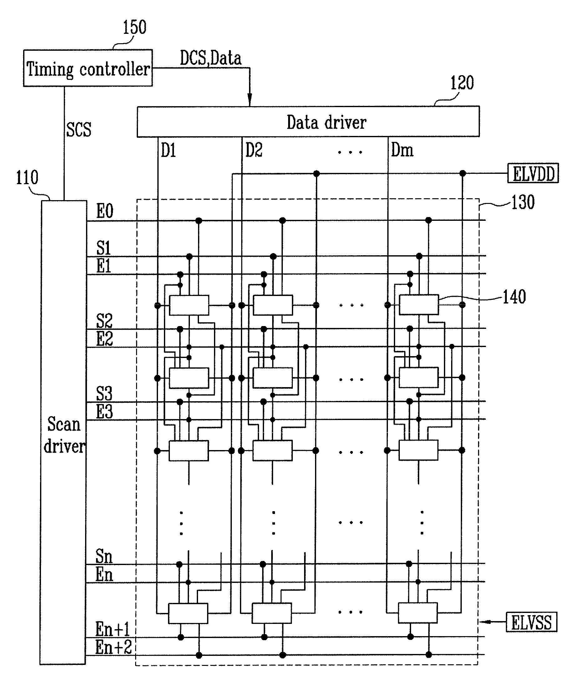
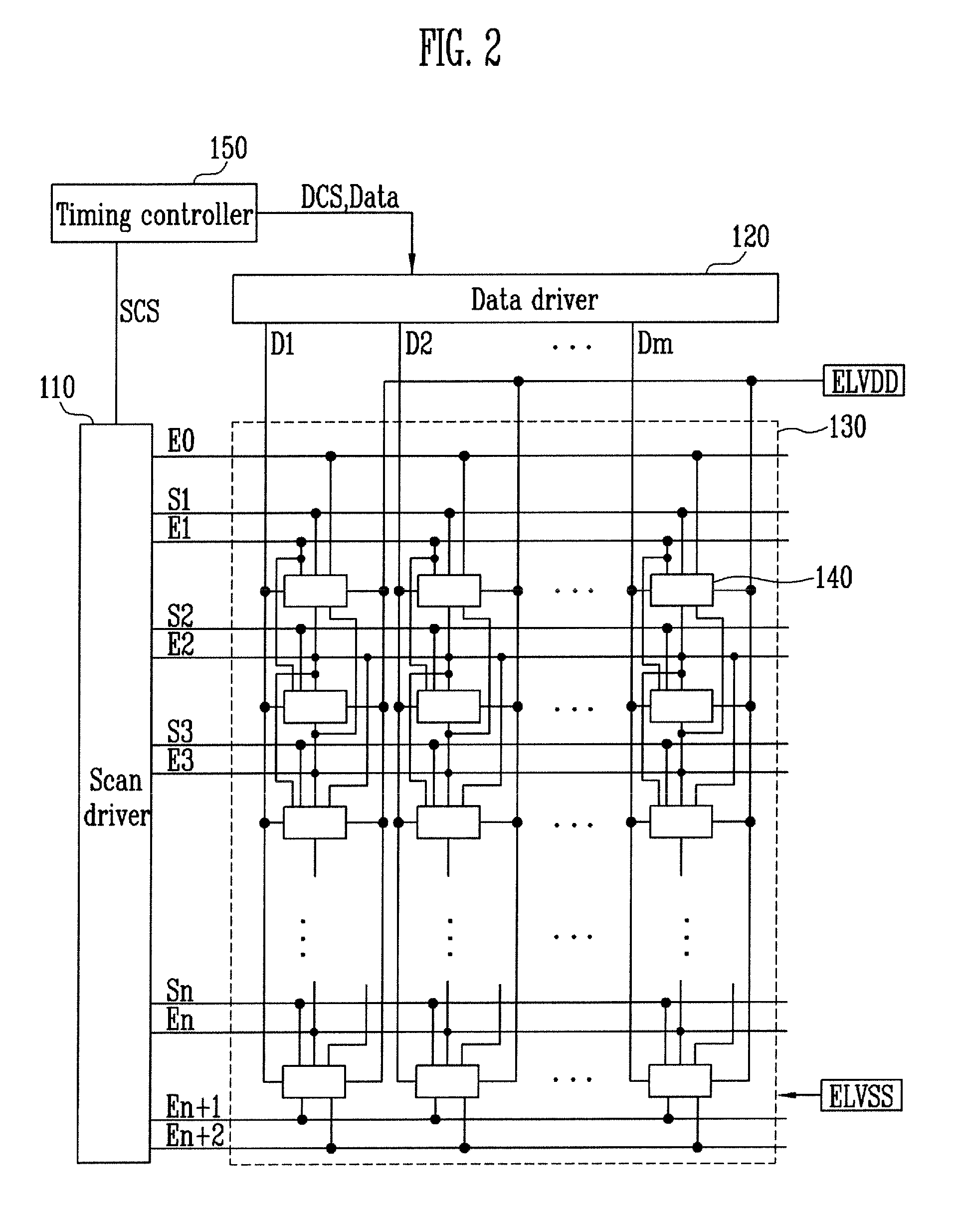
[0023]FIG. 2 illustrates an organic light emitting display according to an embodiment of present invention.

[0024]In FIG. 2, the organic light emitting display according to an embodiment of the present invention includes a display unit 130 including pixels 140 defined by scan lines S1 to Sn, emission control lines E0 to En+2, and data lines D1 to Dm, a scan driver 110 for driving the scan lines S1 to Sn and the emission control ...


PUM


Abstract

A pixel at an ith pixel row (i is a natural number) includes an organic light emitting diode (OLED); a driving transistor for supplying a current to the OLED and a storage capacitor between a gate electrode of the driving transistor and an (i−1)th emission control line; and a compensating unit for controlling a voltage of the gate electrode of the driving transistor to compensate for deterioration of the OLED. The compensating unit includes: a first compensating unit transistor and a second compensating unit transistor between the OLED and a first power source; first and second feedback capacitors between a second node between the first and second compensating unit transistors and a first node between the gate electrode of the driving transistor and the storage capacitor; and a third compensating unit transistor coupled between a third node between the first and second feedback capacitors and a reference voltage source.

Description

CROSS-REFERENCE TO RELATED APPLICATION[0001]This application claims priority to and the benefit of Korean Patent Application No. 10-2007-0126213, filed on Dec. 6, 2007, in the Korean Intellectual Property Office, the entire content of which is incorporated herein by reference.BACKGROUND[0002]1. Field of the Invention[0003]The present invention relates to a pixel and an organic light emitting display including the pixel.[0004]2. Discussion of the Related Art[0005]Recently, various flat panel displays (FPDs) having reduced weight and volume in comparison to cathode ray tubes (CRTs) have been developed. The FPDs include liquid crystal displays (LCDs), field emission displays (FEDs), plasma display panels (PDPs), and organic light emitting displays.[0006]Among the FPDs, the organic light emitting displays display images using organic light emitting diodes (OLEDs) that generate light by re-combination of electrons and holes. The organic light emitting display has high response speed and ...

Claims


Application Information

Patent Timeline
Patent Type & Authority Applications(United States)
IPC IPC(8): G06F3/038
CPCG09G3/3233G09G2300/0814G09G2320/045G09G2310/0262G09G2300/0819G09G3/20G09G3/30G09G3/32H05B33/12
Inventor KIM, DONG-HWIKIM, YANG-WAN
Owner SAMSUNG DISPLAY CO LTD
Why Eureka
Try Eureka