
AMOLED pixel driver circuit and pixel driving method

a pixel driver and pixel driving technology, applied in the field of display techniques, can solve the problems of insufficient compensation function of the 2t1c pixel driver circuit, the necessity of multiple switching, etc., and achieve the effect of reducing the complexity of the data signal, reducing the complexity of the power supply signal, and effective compensating the threshold voltage of the driving

Inactive Publication Date: 2019-06-25
TCL CHINA STAR OPTOELECTRONICS TECH CO LTD
View PDF3 Cites 0 Cited by
  • Summary
  • Abstract
  • Description
  • Claims
  • Application Information

AI Technical Summary

Benefits of technology

This configuration effectively compensates threshold voltage changes, reduces signal complexity, and stabilizes light emission by allowing the data signal to switch only once, enhancing luminance uniformity and display quality.

Problems solved by technology

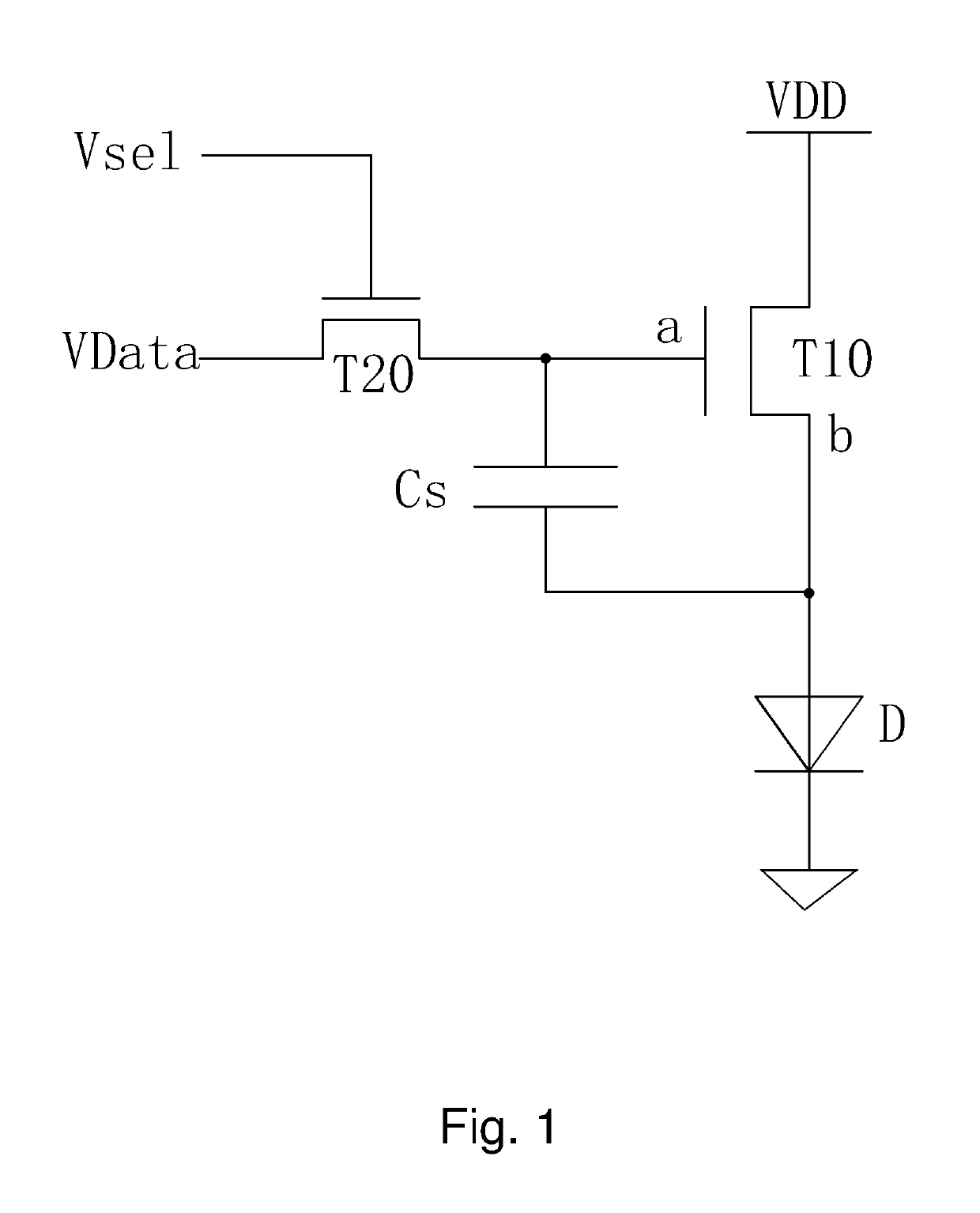
The known AMOLED pixel driver circuit is usually 2T1C structure, that is, two thin film transistors (TFTs) and a capacitor, to convert voltage to current, but the traditional 2T1C pixel driver circuit generally does not provide a compensation function.
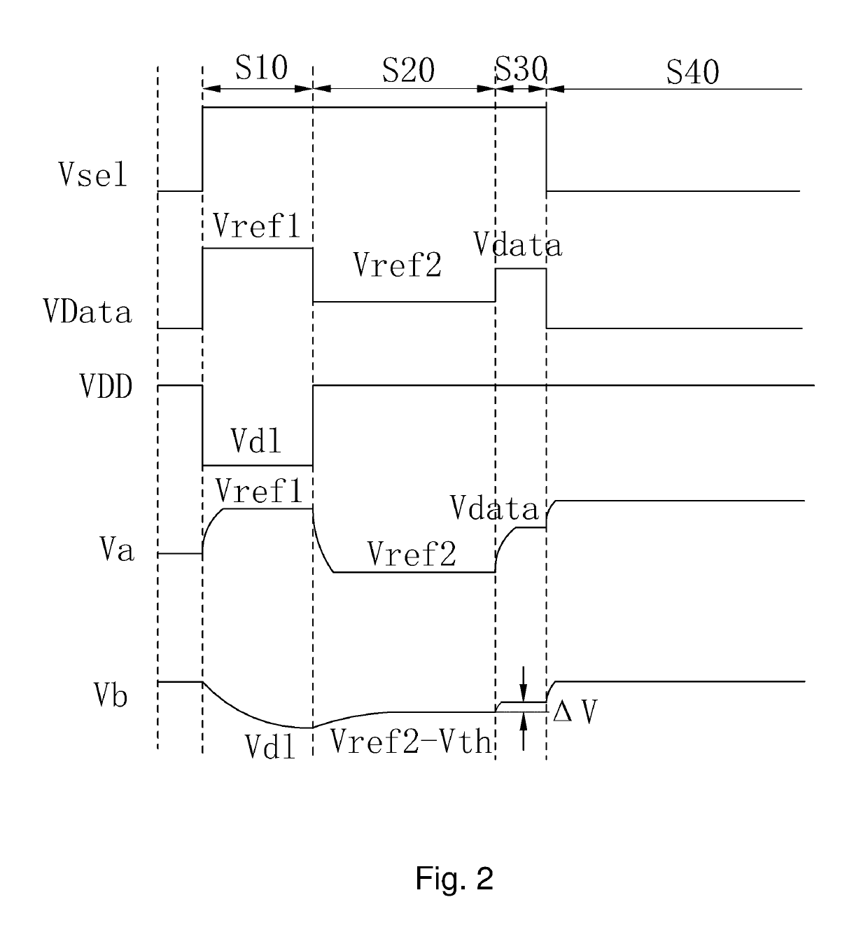
However, as the 2T1C pixel driver circuit shown in FIG. 1, the disadvantages of complex signals of alternating current power supply VDD, complex signals of data signal voltage VData, and the necessity of multiple switching remain issues needed to be addressed.

Method used


Image

  • AMOLED pixel driver circuit and pixel driving method
  • AMOLED pixel driver circuit and pixel driving method
  • AMOLED pixel driver circuit and pixel driving method

Examples


first embodiment

[0093]It should be noted that, in threshold voltage compensation phase S3, the data signal DATA transits from the reference low level Vref to the display data high level Vdata, and cause the influence the source voltage ΔV of the first TFT (i.e., the second node). For the

ΔV=(Vdata−Vref)×(C1 / (C1+COLED)),

wherein COLED is the intrinsic capacitance of the OLED.

[0094]FIG. 4 shows the second embodiment of the AMOLED pixel driver circuit of the present invention. Compared to the first embodiment, the AMOLED pixel driver circuit further comprises a second capacitor C2, with one end connected to the drain of the first TFT T1 and the positive terminal Vdd of the DC power supply, and the other end connected to the source of the first TFT T1 and the second node b. The remaining structure is the same as the first embodiment, and the detailed descriptions will not be repeated here. Furthermore, the second capacitor C2 can be formed by stacking the anode of the OLED OLED and the positive terminal ...

second embodiment

[0095]It should be noted that, in threshold voltage compensation phase S3, the data signal DATA transits from the reference low level Vref to the display data high level Vdata, and cause the influence the source voltage ΔV of the first TFT (i.e., the second node). For the

ΔV=(Vdata−Vref)×(C1 / (C1+C2+COLED)),

wherein COLED is the intrinsic capacitance of the OLED.

[0096]As shown, the second capacitor C2 can regulate the influence on the source voltage of the driving TFT caused by the data signal DATA so as to reduce the complexity of data signal and the data signal only needs to switch once.

[0097]Referring to FIGS. 6-9, in combination with FIGS. 3, 5 or FIGS. 4-5, and based on the AMOLED pixel driver circuit, the present invention also provides an AMOLED pixel driving method, which comprises the following steps:

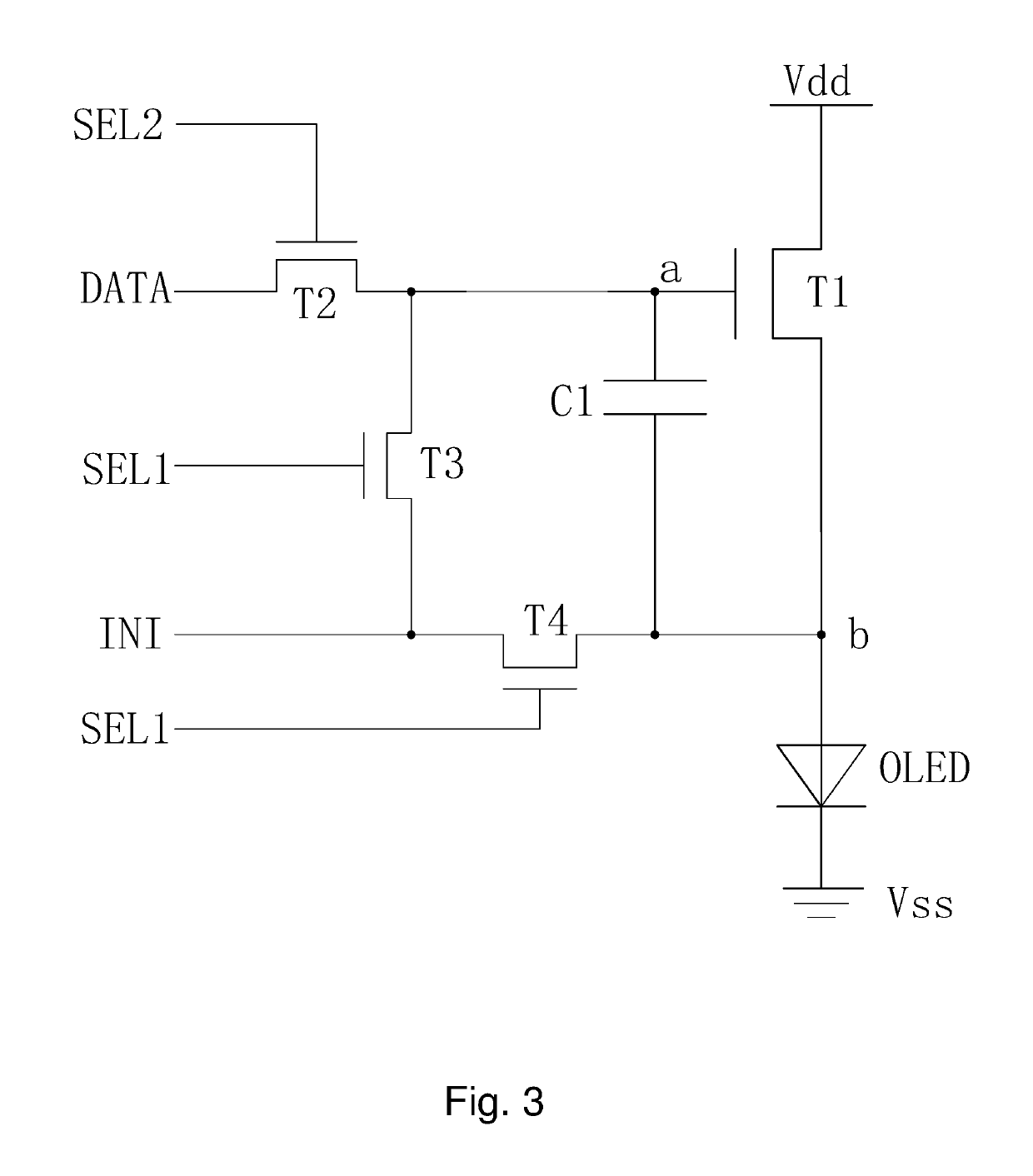
[0098]Step 1: providing an AMOLED pixel driver circuit of 4T1C structure as shown in FIG. 3 or 4T2C structure in FIG. 4. The details of the circuit will not be repeated here.

[0099...


PUM


Abstract

The invention discloses an AMOLED pixel driver circuit and pixel driving method, by using a pixel driver circuit of 4T1C or 4T2C structure to effectively compensate threshold voltage of driving TFT in each pixel; through adding a third TFT (T3) and a fourth TFT (T4) and introducing the first scan signal (SEL1) to control the third TFT (T3) and the fourth TFT (T4) to respectively writing the initialization signal (INI) to initialize the gate and the source of the driving TFT in reset phase so as to reduce the complexity of the power supply signal so that the circuit can use DC power supply directly; by adding a second capacitor (C2) to regulate the influence on the source voltage of the driving TFT by the data signal (DATA) so as to reduce the data signal complexity. As a result, the data signal only needs to switch once.

Description

BACKGROUND OF THE INVENTION1. Field of the Invention[0001]The present invention relates to the field of display techniques, and in particular to an AMOLED pixel driver and pixel driving method.2. The Related Arts[0002]The organic light emitting diode (OLED) display provides the advantages of active light-emitting, low driving voltage, high emission efficiency, quick response time, high resolution and contrast, near 180° viewing angle, wide operation temperature range, and capability to realize flexible display and large-area full-color display, and is regarded as the most promising display technology.[0003]The driving types of OLED can be divided, according to the driving method, into the passive matrix OLED (PMOLED) and active matrix OLED (AMOLED), i.e., the direct addressable type and thin film transistor (TFT) addressable type, wherein the AMOLED provides the advantages of pixels arranged in an array, self-luminous, and high luminous efficiency and is commonly used for high defin...

Claims


Application Information

Patent Timeline
Patent Type & Authority Patents(United States)
IPC IPC(8): G09G3/3258G09G3/3233H01L27/32G09G3/3275G09G3/3266
CPCG09G3/3258G09G3/3233G09G3/3266G09G3/3275H01L27/3265H01L27/3276H01L27/3262G09G2300/0852G09G2300/0819G09G2300/0842H10K59/131H10K59/1213H10K59/1216
Inventor CAI, YUYING
Owner TCL CHINA STAR OPTOELECTRONICS TECH CO LTD
Learn More