

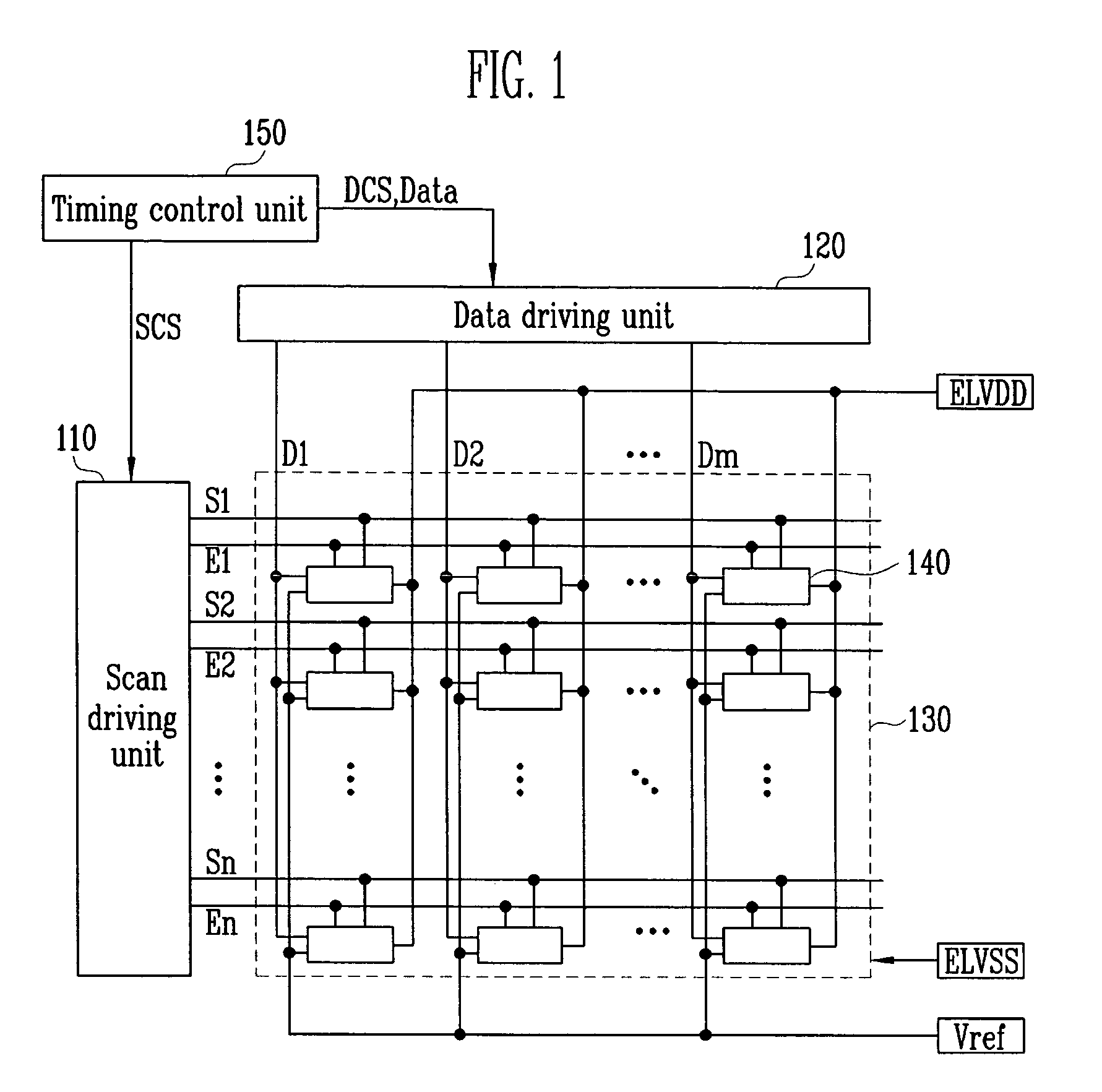
Pixel and organic light emitting display device using the same
a technology of light-emitting display device and pixel, which is applied in the direction of electric digital data processing, instruments, computing, etc., can solve the problem that images having a uniform luminance may not be displayed
- Summary
- Abstract
- Description
- Claims
- Application Information
AI Technical Summary
Benefits of technology
Problems solved by technology
Method used
Image

Examples
first embodiment
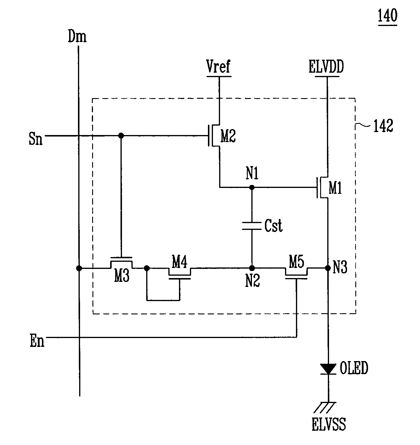
[0044]FIG. 2 illustrates a pixel of in FIG. 1. For convenience of explanation, FIG. 2 shows a pixel 140 coupled to an n-th scan line Sn, an n-th light emitting control line, and an m-th data line Dm.
[0045]Referring to FIG. 2, a pixel 140 according to the first embodiment may include an organic light emitting diode OLED and a pixel circuit 142 coupled to the data line Dm, the scan line Sn, and the light emitting control line En. The pixel circuit 142 may control an amount of current flowing through the organic light emitting diode OLED.
[0046]An anode electrode of the organic light emitting diode OLED may be coupled to the pixel circuit 142, and a cathode electrode of the organic light emitting diode OLED may be coupled to the second power source ELVSS. The organic light emitting diode OLED may generate light having a predetermined luminance in correspondence with an amount of current supplied from the pixel circuit 142.
[0047]When a scan signal is supplied to the pixel circuit 142 thr...
second embodiment
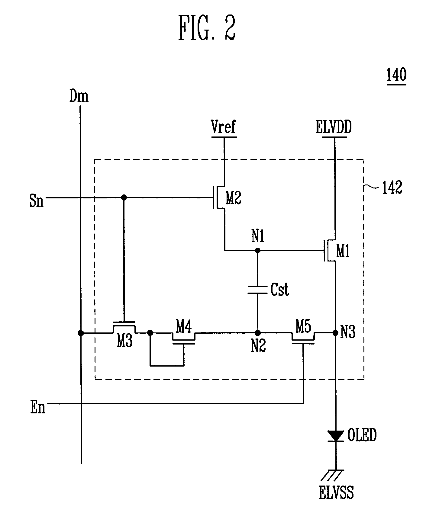
[0066]FIG. 4 illustrates a pixel of FIG. 1. In FIG. 4, elements identical to those of FIG. 2 are provided with the same reference numerals, and the detailed description of such elements will not be repeated.
[0067]Referring to FIG. 4, the pixel 140′ according to the second embodiment may include an organic light emitting diode OLED and a pixel circuit 142′ coupled to the data line Dm, the emission control line En, and the scan line Sn. The pixel circuit 142′ may control an amount of current flowing through the organic light emitting diode OLED.
[0068]The anode electrode of the organic light emitting diode OLED may be coupled to the pixel circuit 142′, and the cathode electrode of the organic light emitting diode OLED may be coupled to the second power source ELVSS. The organic light emitting diode OLED may generate light having a predetermined luminance in correspondence with an amount of current supplied from the pixel circuit 142′.
[0069]When a scan signal is supplied to the pixel ci...
PUM
 Abstract
Description
Claims
Application Information