Semiconductor device and driving method the same

a technology of semiconductor devices and driving methods, applied in the direction of memory adressing/allocation/relocation, instruments, computing, etc., can solve the problems of confusion in the place where such a memory is really used, complicated procedures, etc., to prevent miswriting and tampering of data, reduce the occurrence of causing defects such as writing defects, and improve the reliability of wireless communication between the rfid tag and the communication device or the lik

Inactive Publication Date: 2011-03-03
SEMICON ENERGY LAB CO LTD
View PDF16 Cites 1 Cited by
  • Summary
  • Abstract
  • Description
  • Claims
  • Application Information

AI Technical Summary

Benefits of technology

[0013]In view of the foregoing problem, it is an object to prevent miswriting by radio in a relatively easy way in a semiconductor device which is capable of data communication (reception / transmission) through wireless communication, in particular, in an RFID tag provided with an OTP memory or a write-once memory. Alternatively, it is an object to prevent information from being tampered. Further alternatively, it is an object to inhibit access to a memory in a relatively easy way and to inhibit reading of information in a semiconductor device which is capable of data communication (reception / transmission) through wireless communication.
[0029]Therefore, when data for preventing additional writing is written to the sector for preventing additional writing of the memory included in the semiconductor device, information is written to the information sector which is electrically connected to the sector for preventing additional writing, and the information is held, written information is confirmed and additional writing becomes impossible. Accordingly, miswriting and tampering of data are prevented.
[0030]Further, when a sector for determining whether writing is possible is provided for the memory, it is confirmed that information is not surely written to the information sector, and correct information can be accurately written at the time of writing to the information sector, whereby occurrence of causing defects such as writing defects is reduced, and reliability of wireless communication between the RFID tag and a communication device or the like is improved.
[0031]Therefore, reliability of the RFID tag is improved when the sector for preventing additional writing and the sector for determining whether writing is possible are provided.
[0032]In the case where a sector for inhibiting writing is used instead of the sector for preventing additional writing, data for inhibiting writing is written to the sector for inhibiting writing, information is written to the information sector electrically connected to the sector for inhibiting writing, and the information is held. Further, when data for inhibiting writing is written to the sector for inhibiting writing, access to the memory can be completely interrupted. Thus, data which becomes unnecessary is prevented from being leaked.

Problems solved by technology

Patent Document 1 is effective for preventing data from being tampered, but a procedure is complicated because a damaging process is included; therefore, a place where such a memory is really used might be confused.

Method used


Image

  • Semiconductor device and driving method the same
  • Semiconductor device and driving method the same
  • Semiconductor device and driving method the same

Examples


embodiment 1

[0062]In this embodiment, a configuration of a semiconductor device of one embodiment of the present invention that is capable of communicating data through wireless communication will be described.

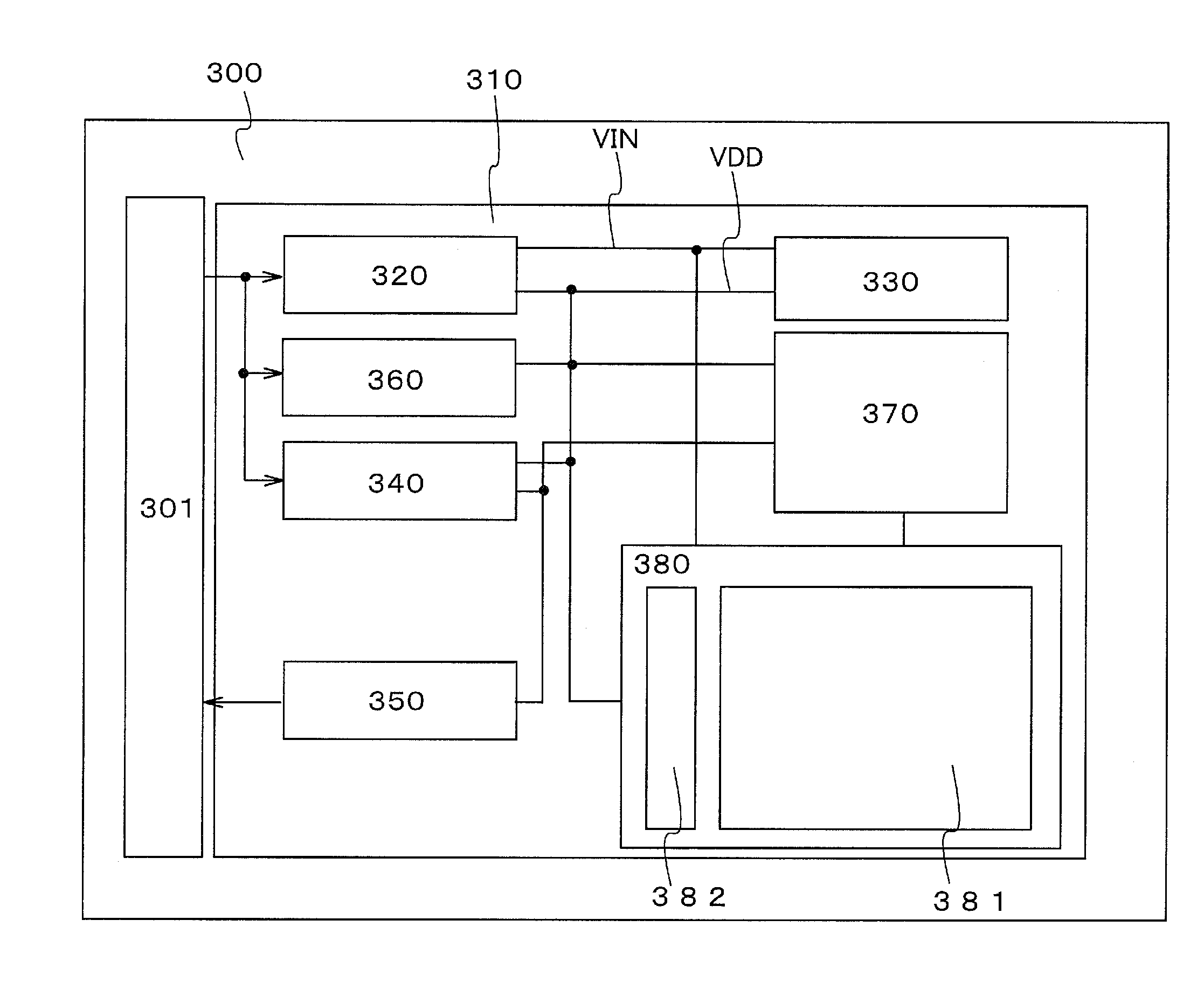
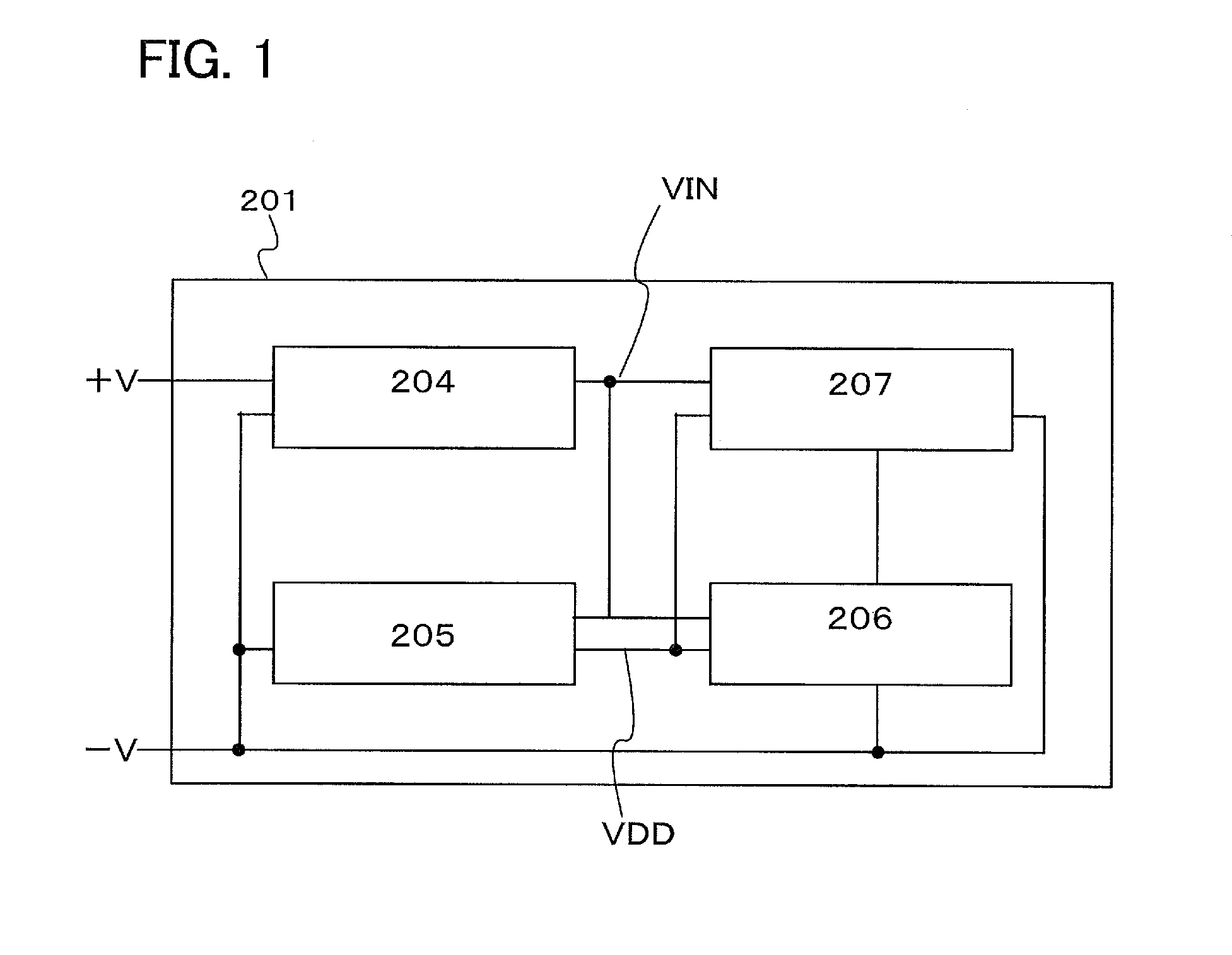
[0063]As illustrated in FIG. 1, a semiconductor device 201 includes an input circuit 204, a circuit 205 which generates a constant voltage, a control circuit 206, and an OTP memory or write-once memory (hereinafter referred to as a memory) 207. In this embodiment, an RFID tag using the semiconductor device 201 in FIG. 1 will be described with reference to FIG. 3. As illustrated in FIG. 3, the case where a memory 380 includes an information sector 381 and a sector for preventing additional writing 382 is described. The information sector 381 and the sector for preventing additional writing 382 are electrically connected to each other.

[0064]An input circuit 320 rectifies an input AC signal to generate a DC voltage. Any circuit configuration can be employed as long as the circuit rectifies a...

embodiment 2

[0081]In this embodiment, a structure of a semiconductor device of one embodiment of the present invention which can perform data communication through wireless communication and which is different from the structure described in Embodiment 1 will be described.

[0082]As illustrated in FIG. 1, the semiconductor device 201 includes the input circuit 204, the circuit 205 which generates a constant voltage, the control circuit 206, and the memory 207. In Embodiment 2, an RFID tag using the semiconductor device 201 in FIG. 1 will be described with reference to FIG. 4. As illustrated in FIG. 4, the case where the memory 380 includes the information sector 381, the sector for preventing additional writing 382, and a sector for determining whether writing is possible 383 is described. A semiconductor integrated circuit illustrated in FIG. 4 is the same as the semiconductor integrated circuit described in Embodiment 1 except the structure of the memory. Note that the information sector 381, t...

embodiment 3

[0101]In this embodiment, a structure and operation of a semiconductor device of one embodiment of the present invention when it is provided for an RFID tag will be described.

[0102]A schematic view of a wireless communication system is illustrated in FIG. 9. The wireless communication system mainly includes a communication device 3010, an antenna unit 3020 which is electrically connected to the communication device 3010, an RFID tag 300, and a controlling terminal 3030 which controls the communication device.

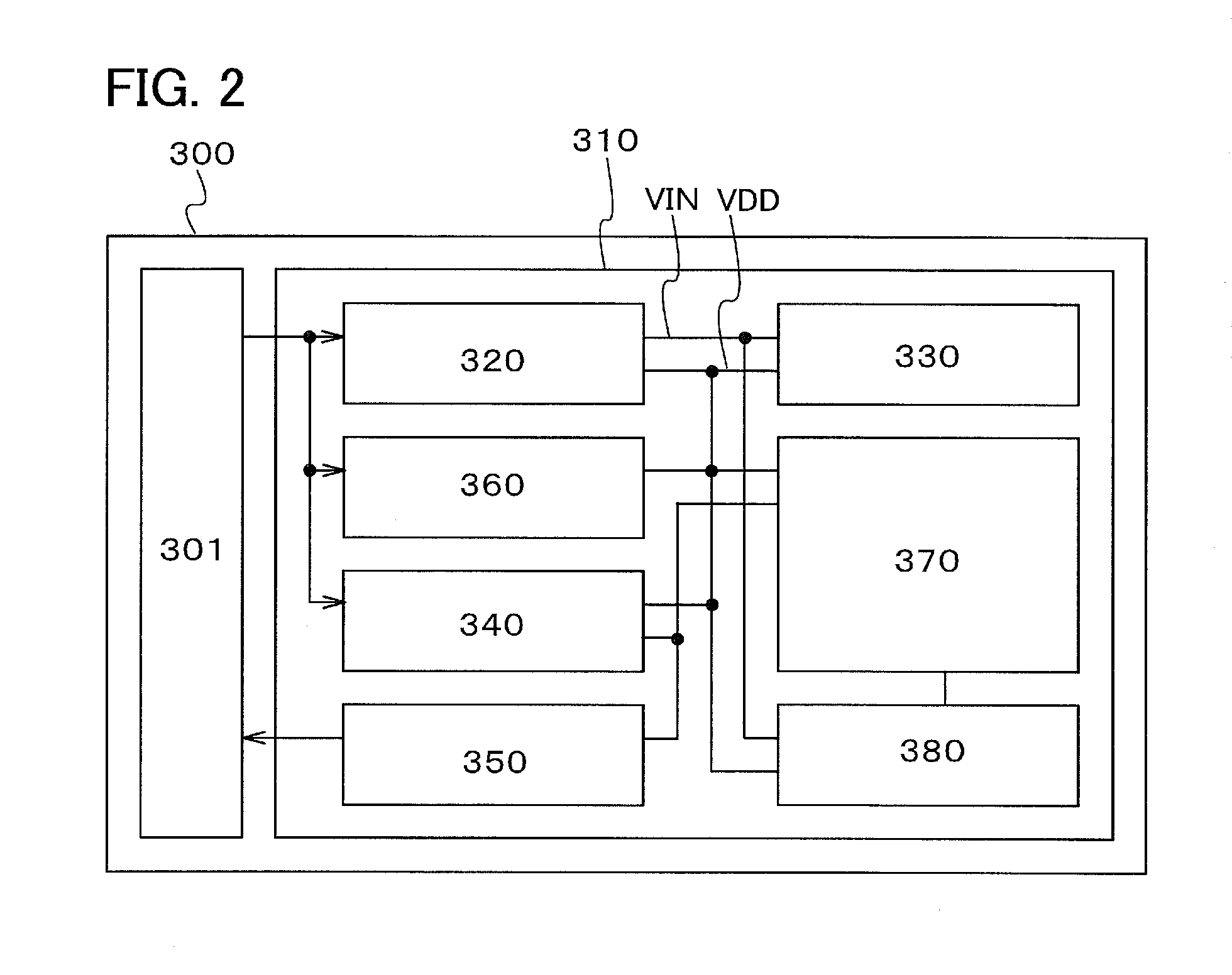
[0103]A circuit configuration of the RFID tag 300 is illustrated in FIG. 2. The RFID tag 300 includes an antenna 301 and the semiconductor integrated circuit 310. Although not illustrated, the antenna 301 may be provided in the semiconductor integrated circuit 310 or may be provided outside the semiconductor integrated circuit 310 as illustrated in FIG. 2. The semiconductor integrated circuit 310 includes the input circuit 320, the circuit 330 which generates a constant voltage,...


PUM


Abstract

It is an object to prevent miswriting by radio in a relatively easy way in a semiconductor device which is capable of data communication (reception / transmission) through wireless communication, in particular, in an RFID tag provided with an OTP memory or a write-once memory. Alternatively, it is an object to prevent data from being tampered. Further alternatively, it is an object to inhibit access to a memory in a relatively easy way and to inhibit reading of data in a semiconductor device which is capable of data communication (reception / transmission) through wireless communication. In a semiconductor device including a control circuit and an OTP memory, a memory includes at least a sector for preventing additional writing and an information sector. When data for preventing additional writing is written to the sector for preventing additional writing and information is written to the information sector which is electrically connected to the sector for preventing additional writing, additional writing to the information sector to which the information is written is impossible.

Description

BACKGROUND OF THE INVENTION[0001]1. Field of the Invention[0002]The present invention relates to a semiconductor device which is capable of data communication (reception / transmission) through wireless communication and a driving method thereof.[0003]2. Description of the Related Art[0004]In recent days, an individual identification technique using wireless communication (hereinafter referred to as a wireless communication system) has attracted attention. Specifically, RFID tags (also referred to as IC tags, IC chips, RF tags, wireless tags, or electronic tags) have begun to be used for production, management, and the like of individual objects. In addition, the RFID tags are expected to be used for personal authentication.[0005]The wireless communication system is a system in which data communication is performed by wireless communication between a transmitter / receiver serving also as a power supply source or a transmitter / receiver such as a communication device (also referred to as...

Claims


Application Information

Patent Timeline
Patent Type & Authority Applications(United States)
IPC IPC(8): G06F12/00G06F12/02
CPCG06F2212/178G06F12/1433G06K19/073G06K19/077
Inventor ISHII, MASATOTAKAHASHI, YASUYUKIOHMARU, TAKUROKOBAYASHI, HIDETOMOSHIONOIRI, YUTAKA
Owner SEMICON ENERGY LAB CO LTD
Why Eureka
Try Eureka