Unlock instant, AI-driven research and patent intelligence for your innovation.

Digital circuit block having reducing supply voltage drop and method for constructing the same

a digital circuit and supply voltage drop technology, applied in the direction of dc circuit to reduce harmonics/ripples, electric variable regulation, instruments, etc., can solve the problems of significant leakage current induced, electric charge may leak from the gate terminal to the substrate of the cmos transistor, etc., to and reduce the supply voltage drop

Active Publication Date: 2012-03-08
MEDIATEK INC
View PDF12 Cites 0 Cited by
  • Summary
  • Abstract
  • Description
  • Claims
  • Application Information

AI Technical Summary

Benefits of technology

[0005]According to an embodiment of the present invention, a digital circuit block having reducing supply voltage drop is provided. The digital circuit block comprises a first conducting segment having a first end coupled to a first supply voltage; a second conducting segment having a first end coupled to a second supply voltage; a digital logic coupled between a second end of the first conducting segment and a second end of the second conducting segment; a first conducting layer; a second conducting layer, wherein the first conducting layer and the second conducting layer are different depth layers; a dielectric layer being between the first conducting layer and the second conducting layer; a third conducting segment, having a first end electrically connected to the first conducting segment, a second end not electrically connected to the second conducting segment, and a first portion located at the first conducting layer; and a fourth conducting segment, having a first end electrically connected to the second conducting segment, a second end not electrically connected to the first conducting segment, and a second portion located at the second conducting layer; wherein the first portion, the second portion, and the dielectric layer form a first capacitive element to reduce the supply voltage drop between the first supply voltage and the second supply voltage.
[0006]According to a second embodiment of the present invention, a method for constructing a digital circuit block having reducing supply voltage drop is provided, wherein the digital circuit block comprises a first conducting segment having a first end coupled to a first supply voltage, a second conducting segment having a first end coupled to a second supply voltage, a digital logic coupled between a second end of the first conducting segment and a second end of the second conducting segment, a first conducting layer, a second conducting layer, and a dielectric layer being between the first conducting layer and the second conducting layer, the method comprising: constructing a third conducting segment having a first end electrically connected to the first conducting segment, a second end not electrically connected to the second conducting segment, and a first portion located at the first conducting layer; wherein the first conducting layer and the second conducting layer are different depth layers; and constructing a fourth conducting segment having a first end electrically connected to the second conducting segment, a second end not electrically connected to the first conducting segment, and a second portion located at the second conducting layer; wherein the first portion, the second portion, and the dielectric layer form a first capacitive element to reduce the supply voltage drop between the first supply voltage and the second supply voltage.

Problems solved by technology

However, since the filler capacitor 15 is implemented by a CMOS (Complementary Metal Oxide Semiconductor) transistor, and the electric charge of the filler capacitor is accumulated on the gate terminal and the substrate of the CMOS transistor, the electric charge may leak from the gate terminal to the substrate of the CMOS transistor.
Therefore, a significant leakage current may be induced if the digital circuit 10 includes a large number of filler capacitors.

Method used


Image

  • Digital circuit block having reducing supply voltage drop and method for constructing the same
  • Digital circuit block having reducing supply voltage drop and method for constructing the same
  • Digital circuit block having reducing supply voltage drop and method for constructing the same

Examples


Embodiment Construction

[0013]Certain terms are used throughout the description and following claims to refer to particular components. As one skilled in the art will appreciate, manufacturers may refer to a component by different names. This document does not intend to distinguish between components that differ in name but not function. In the following description and in the claims, the terms “include” and “comprise” are used in an open-ended fashion, and thus should be interpreted to mean “include, but not limited to . . . ”. Also, the term “couple” is intended to mean either an indirect or direct electrical connection. Accordingly, if one device is coupled to another device, that connection may be through a direct electrical connection, or through an indirect electrical connection via other devices and connections.

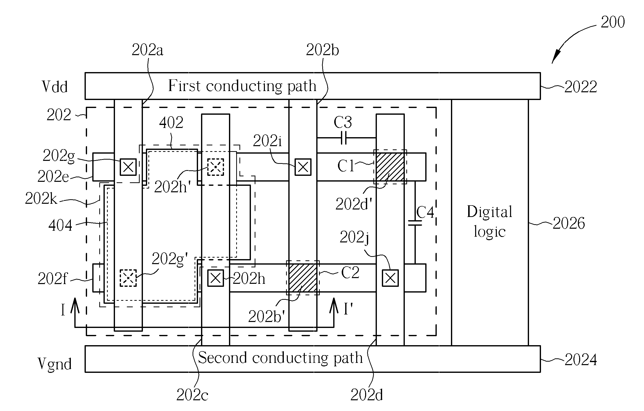
[0014]Please refer to FIG. 2 in conjunction with FIG. 3. FIG. 2 is a top view diagram illustrating a layout architecture 202 for reducing a supply voltage drop in a digital circuit block 200 ...


PUM

PropertyMeasurementUnit
supply voltage dropaaaaaaaaaa
supply voltageaaaaaaaaaa
depthaaaaaaaaaa

Abstract

A digital circuit block includes first to fourth conducting segments, a digital logic, first and second conducting layers, and a dielectric layer. The first and second conducting segments are coupled to first and second supply voltages, respectively. The digital logic and dielectric layer are between the first and second conducting segments. The third conducting segment includes a first end electrically connected to the first conducting segment, a second end not electrically connected to the second conducting segment, and a first portion located at the first conducting layer. The fourth conducting segment includes a first end electrically connected to the second conducting segment, a second end not electrically connected to the first conducting segment, and a second portion located at the second conducting layer. The first and second portions and dielectric layer are formed a first capacitive element to reduce the supply voltage drop between the first and second supply voltages.

Description

CROSS REFERENCE TO RELATED APPLICATIONS[0001]This application is a Continuation application of co-pending U.S. patent application Ser. No. 12 / 358,215, which was filed on Jan. 22, 2009 and is incorporated herein by reference.BACKGROUND OF THE INVENTION[0002]The present invention is related to supplying a supply voltage to a digital circuit, and more particularly, to a digital circuit block having reducing supply voltage drop and a method for constructing the same.[0003]In the field of digital circuit design, one of the most efficient ways to arrange each of the digital cells within a digital circuit is to perform an automatic placement and routing (APR) process upon the functional digital cells after the digital circuit is designed. Normally, the APR process is performed by software tools. Please refer to FIG. 1. FIG. 1 is a diagram illustrating a prior art digital circuit 10 after performing the APR process. The digital circuit 10 comprises a plurality of functional digital cells 11...

Claims


Application Information

Patent Timeline
Patent Type & Authority Applications(United States)
IPC IPC(8): H02J1/02H05K3/00
CPCH01L27/0207H01L23/5286H01L23/5223H03K19/00346Y10T29/49124H01L2924/0002H01L28/20H01L2924/00
Inventor HUANG, SHEN-YULIN, CHIH-CHING
Owner MEDIATEK INC