Display device

Active Publication Date: 2012-05-17
GLOBAL OLED TECH
View PDF1 Cites 7 Cited by
  • Summary
  • Abstract
  • Description
  • Claims
  • Application Information

AI Technical Summary

Benefits of technology

[0015]Further, it is preferred that, in the display device according to the present invention, when defining that a shortest sub-frame period among the plurality of sub-frame periods is 1, each frame be constituted by one sub-frame having a length of 2k, where k is 0 to N−3, and three sub-frames each having

Problems solved by technology

In a thin film transistor (TFT) formed on a glass substrate, especially a low-temperature polysilicon (LIPS) TFT, the values of the threshold voltage Vth and the mobility μ are varied among pixels, resulting in a problem of uneven display.
The voltage-driven type device illustrated in FIG. 1 as the related art has a problem of screen burn-in because luminance becomes lowered as the current amount is reduced by the influence of voltage rise due to the temporal change in the organic EL element.
There is another problem that the luminance depends on pixel positions and becomes uneven because of the currents flowing through the organic EL elements i

Method used


Image

  • Display device
  • Display device
  • Display device

Examples


embodiment

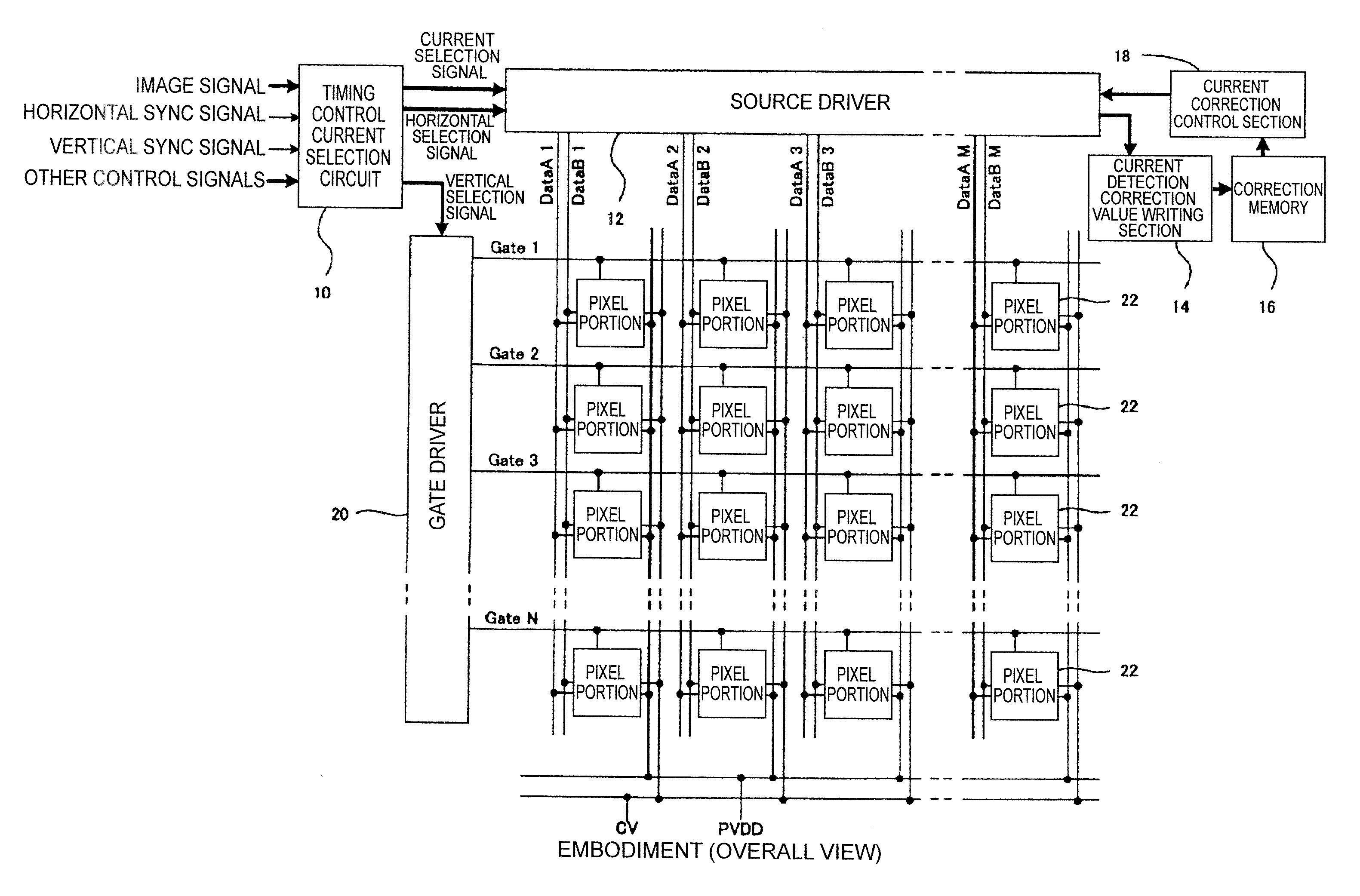
[0036]FIG. 3 illustrates an overall configuration of a display device as an embodiment. FIG. 4 illustrates a configuration of one pixel portion and a configuration of a source driver for one line.

[0037]As illustrated in FIG. 3, an image signal, a horizontal synchronization signal, a vertical synchronization signal, and other control signals are supplied to a timing control current selection circuit 10. A current selection signal indicating image data (bit data) of each pixel and a horizontal control signal indicating its timing are generated based on the image signal, the horizontal synchronization signal, and the like, and then supplied to a source driver 12.

[0038]The source driver 12 is connected to a current detection correction value writing section 14. The current detection correction value writing section 14 detects each current value of current sources provided for each column in the source driver 12 as described later, and determines a correction value therefor. The current ...


PUM


Abstract

Display unevenness is suppressed. A display device includes pixels (22) arranged in matrix, each including a current-driven type light emitting element (EL) and a drive transistor (Tr3) for supplying a current to the current-driven type light emitting element (EL). The current-driven type light emitting element (EL) is driven by dividing each frame period into a plurality of sub-frame periods for lighting time. The drive transistor is controlled under current write driving using two write currents having a ratio of 1:1/2N and a sum of the two write currents.

Description

[0001]The present invention claims the benefit of Japanese Patent Application No. 2010-23287, filed in Japan on Feb. 4, 2010, which is hereby incorporated by reference.BACKGROUND OF THE INVENTION[0002]1. Field of the Invention[0003]The present invention relates to a display device in which pixel data for display is written into each pixel arranged in matrix, and to a drive method for the display device.[0004]2. Description of the Related Art[0005]There have been proposed various types of display devices, typified by the one disclosed in Japanese Patent Application Laid-open No. 1998-214060, in which gradation display is performed by dividing each frame period into a plurality of sub-frame periods for driving.[0006]FIG. 1 illustrates a configuration of a circuit of one pixel (pixel circuit) in an organic electroluminescence (EL) display device of time-division gradation display mode disclosed in Japanese Patent Application Laid-open No. 1998-214060. In a simple 2T-1C configuration (i...

Claims


Application Information

Patent Timeline
IPC IPC(8): G09G5/00
CPCG09G3/2033G09G3/2081G09G2310/0251G09G2310/0262G09G2320/0252G09G2320/0266G09G3/3233G09G2300/0842G09G2320/0233G09G2320/0261G09G3/30
Inventor KOHNO, MAKOTOMORI, NOBUYUKIMIZUKOSHI, SEIICHI
Owner GLOBAL OLED TECH
Why Eureka
Try Eureka