Method for driving display device, display device, and electronic device

a display device and electronic device technology, applied in the field of display devices, can solve the problems of low display image quality, display defect, degraded display image reproducibility, etc., and achieve the effects of improving color reproducibility of display image, preventing image quality degradation of display image, and improving display image quality

Inactive Publication Date: 2013-09-12
SEMICON ENERGY LAB CO LTD
View PDF10 Cites 5 Cited by
  • Summary
  • Abstract
  • Description
  • Claims
  • Application Information

AI Technical Summary

Benefits of technology

[0018]According to one embodiment of the present invention, degradation in image quality of a display image can be prevented.
[0019]For example, according to one embodiment of the present invention, a pixel circuit to which image data cor

Problems solved by technology

A display device using a conventional field-sequential method has a problem of low quality of a display im

Method used


Image

  • Method for driving display device, display device, and electronic device
  • Method for driving display device, display device, and electronic device
  • Method for driving display device, display device, and electronic device

Examples


embodiment 1

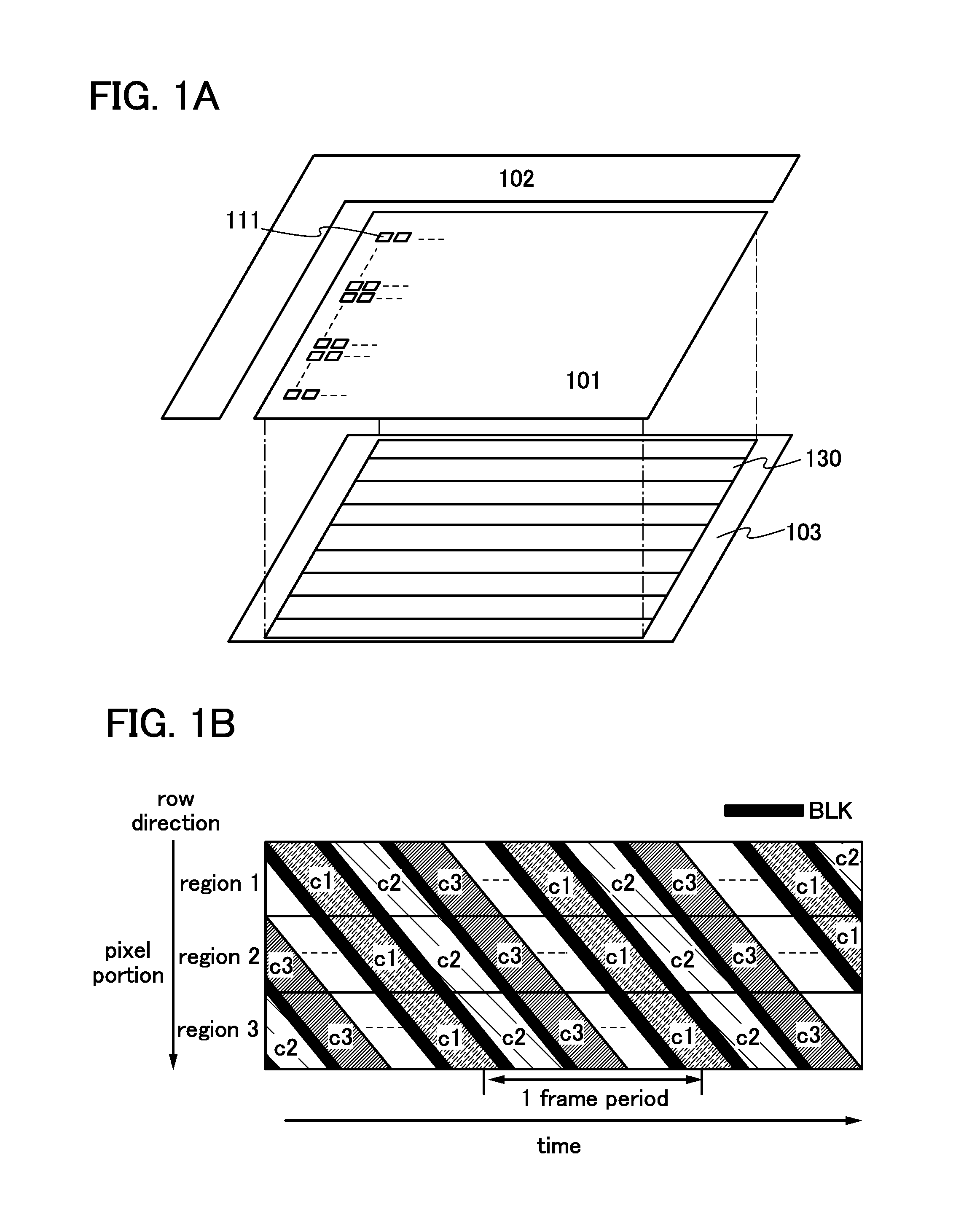
[0037]In this embodiment, examples of a field-sequential display device will be described.

[0038]FIG. 1A is a block diagram illustrating a structural example of a display device of this embodiment.

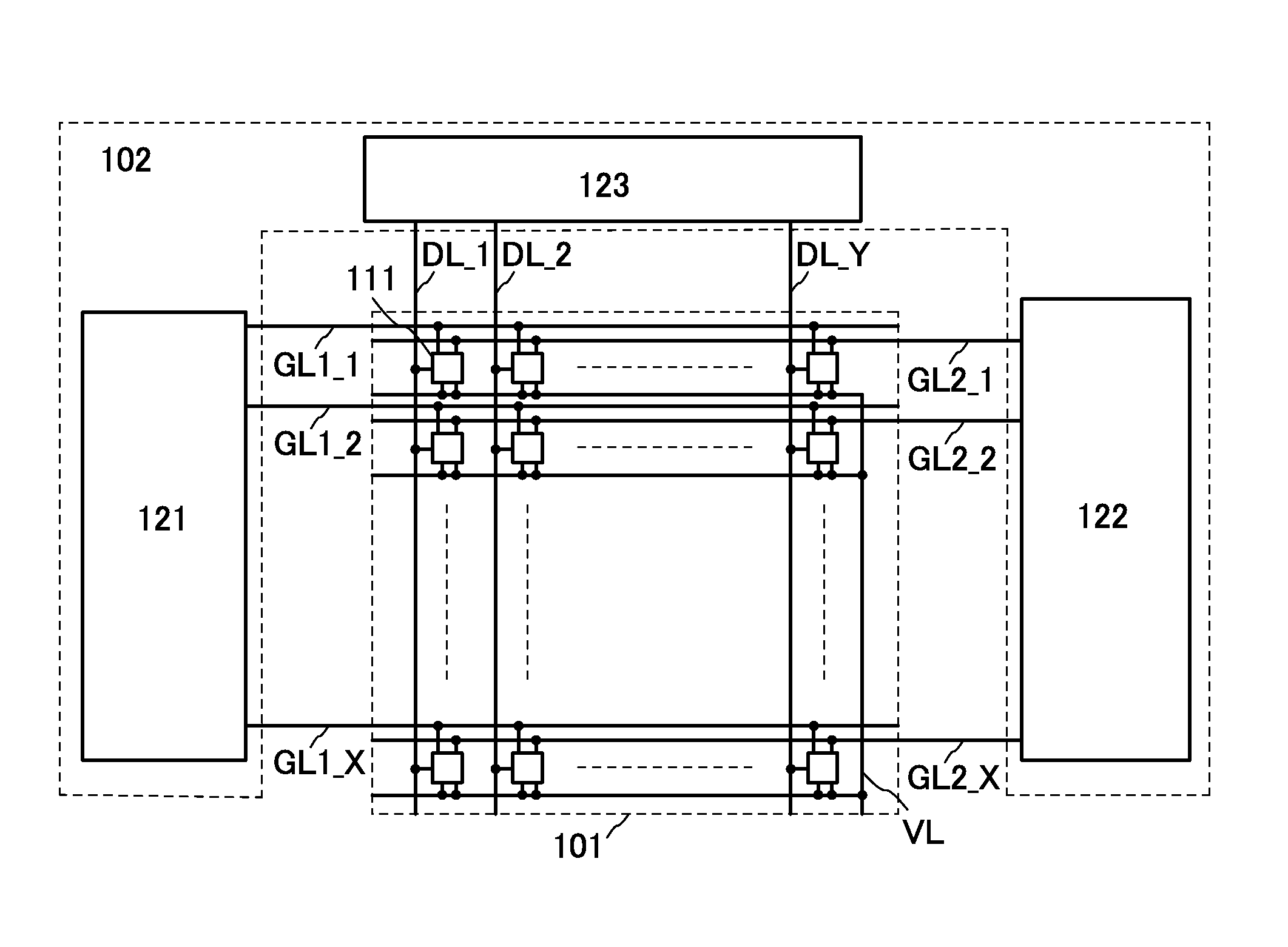
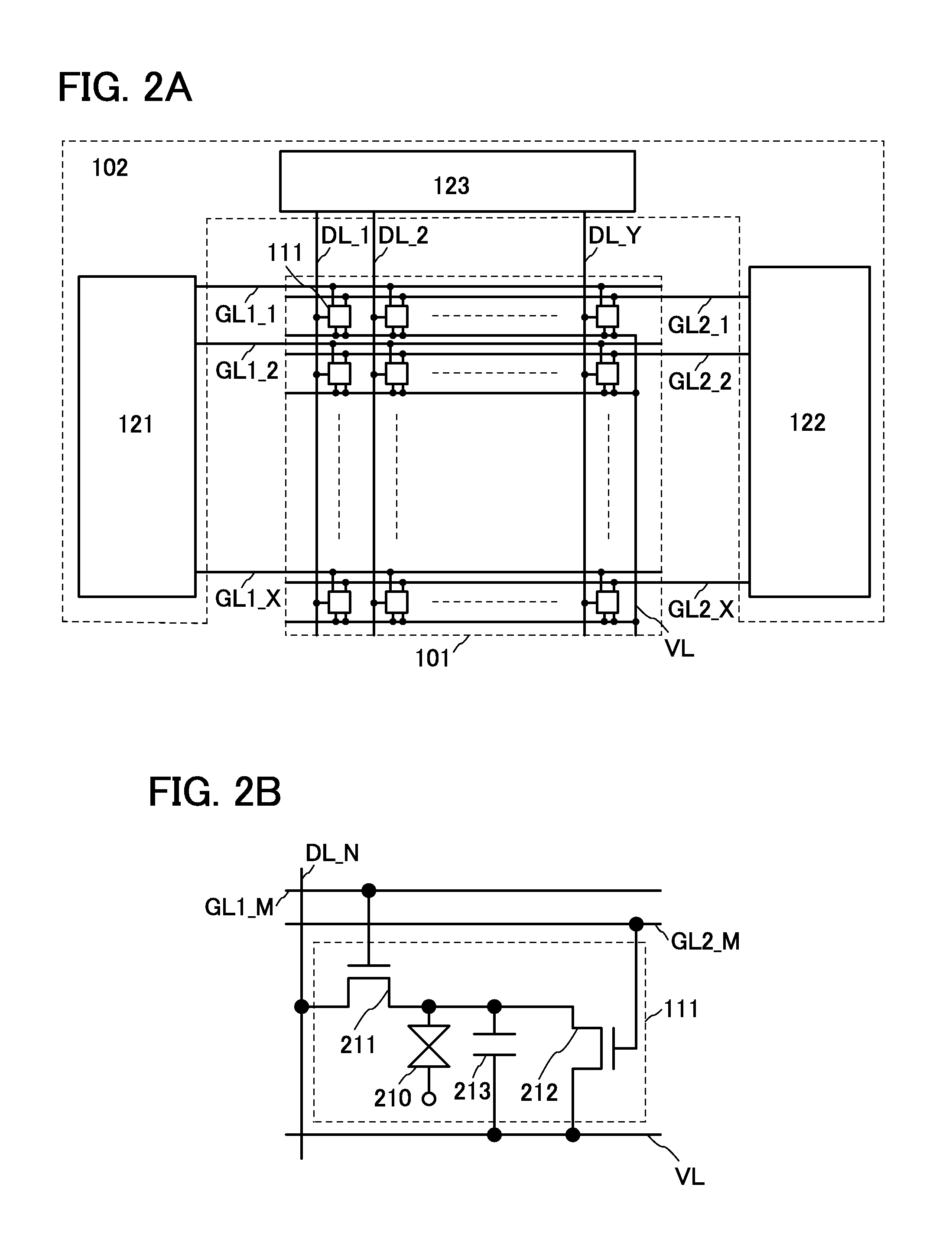
[0039]The display device in FIG. 1A includes a pixel portion 101, a driver circuit portion 102, and a light source portion 103. Note that the driver circuit portion 102 and the light source portion 103 are not necessarily provided inside the display device.

[0040]The pixel portion 101 includes a plurality of pixel circuits 111 arranged in the row and column directions.

[0041]Data is written to the pixel circuits 111, and the pixel circuits 111 change their display states according to the written data.

[0042]The pixel portion 101 is divided into a plurality of regions in the row direction. The driver circuit portion 102 has a function of controlling writing of data to the pixel circuits 111 in each of the plurality of regions.

[0043]In the light source portion 103, each of the plurality of regio...

embodiment 2

[0180]In this embodiment, a structural example of a display device will be described with reference to FIG. 13.

[0181]An example of the display device of this embodiment is a liquid crystal display device of a horizontal electric field mode, and includes conductive layers 701a to 701c, an insulating layer 702, semiconductor layers 703a and 703b, conductive layers 704a to 704d, an insulating layer 705, an insulating layer 707, a conductive layer 709, a conductive layer 710, an insulating layer 722, an insulating layer 723, and a liquid crystal layer 750, as illustrated in FIG. 13.

[0182]The conductive layers 701a to 701c are provided on one surface of a substrate 700.

[0183]The conductive layer 701a is provided in the driver circuit portion 102 illustrated in FIG. 1A. The conductive layer 701a serves as a gate of a transistor in a driver circuit.

[0184]The conductive layer 701b is provided in the pixel portion 101 illustrated in FIG. 1A. The conductive layer 701b serves as a gate of a tr...

embodiment 3

[0244]In this embodiment, examples of an electronic device including a panel which uses a display device according to one embodiment of the present invention will be described with reference to FIGS. 14A to 14D.

[0245]The electronic device illustrated in FIG. 14A is an example of a portable information terminal.

[0246]The electronic device illustrated in FIG. 14A includes a housing 1011, a panel 1012 incorporated in the housing 1011, a button 1013, and a speaker 1014.

[0247]The housing 1011 may be provided with a connection terminal for connecting the electronic device to an external device and a button for operating the electronic device.

[0248]The panel 1012 is a display panel (display) and preferably has a function of a touch panel.

[0249]The panel 1012 is formed using a display device according to one embodiment of the present invention.

[0250]The button 1013 is provided on the housing 1011. For example, when the button 1013 is a power button, pressing the button 1013 can turn on or o...


PUM


Abstract

Degradation in image quality of a display image is prevented. A pixel portion which includes a plurality of pixel circuits in row and column directions is divided into a plurality of regions in the row direction. In each of the plurality of regions, operation in which data is written to the pixel circuits on a row basis and the pixel circuits to which the data is written are irradiated with light corresponding to the written data is performed a plurality of times in one frame period in such a manner that at least three single-color image data for displaying the three primary colors are written in one frame period; and black image data is written to the pixel circuits every time before any of the plurality of single-color image data is written to the pixel circuits in each of the plurality of regions.

Description

BACKGROUND OF THE INVENTION[0001]1. Field of the Invention[0002]One embodiment of the present invention relates to a display device. Further, one embodiment of the present invention relates to an electronic device including a panel which uses the display device.[0003]2. Description of the Related Art[0004]In recent years, a display device using a method in which the color of light transmitted to a pixel circuit is changed a plurality of times in one frame period so that a full-color image can be displayed (such a method is referred to as a field-sequential method) has been developed (for example, see Patent Document 1). When a field-sequential method is employed, for example, a color filter is not needed in a liquid crystal display device, and thus, light transmittance can be increased.[0005]In a display device using a field-sequential method in Patent Document 1, a pixel portion including pixel circuits in the row and column directions is divided into a plurality of regions in the ...

Claims


Application Information

Patent Timeline
IPC IPC(8): G09G5/02
CPCG09G3/3659G09G2310/0235G09G3/3607G09G2310/063G09G5/02G09G2310/0237G09G3/36
Inventor MIYAKE, HIROYUKI
Owner SEMICON ENERGY LAB CO LTD
Why Eureka
Try Eureka