Display device, display module, and electronic device

a display module and display device technology, applied in semiconductor devices, instruments, computing, etc., can solve problems such as display quality decline, and achieve the effect of high display quality and thinness reduction

Inactive Publication Date: 2015-10-22
SEMICON ENERGY LAB CO LTD
View PDF8 Cites 32 Cited by
  • Summary
  • Abstract
  • Description
  • Claims
  • Application Information

AI Technical Summary

Benefits of technology

[0017]One embodiment of the present invention can provide a display device or the like having a novel structure.
[0018]One embodiment of the present invention can provide a display device or the like having a novel structure with which thickness reduction can be achieved. One embodiment of the present invention can provide a display device or the like having a novel structure with which a change in a potential applied to a display element can be canceled. Therefore, a display device having high display quality can be obtained.

Problems solved by technology

When the housing is thinned, a potential supplied to a display element is changed by a signal supplied to an electrode, which decreases display quality.

Method used


Image

  • Display device, display module, and electronic device
  • Display device, display module, and electronic device
  • Display device, display module, and electronic device

Examples


embodiment 1

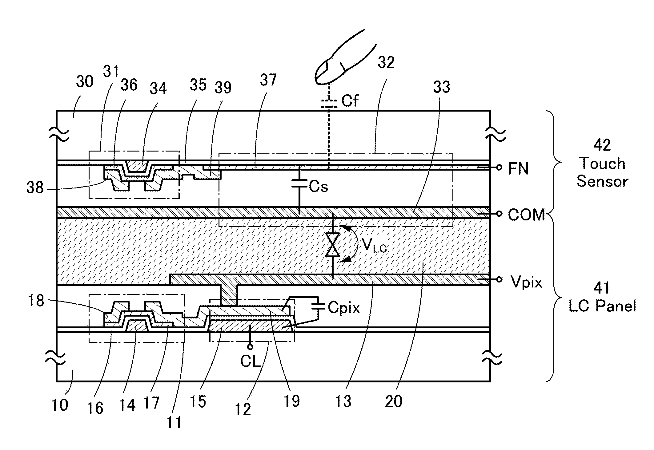
[0052]In this embodiment, a structure example of a display device and the operation of the display device is described.

[0053]In this specification and the like, a display device refers to a device including a display element such as a liquid crystal element. Note that the display device also includes a driver circuit for driving a plurality of pixels, and the like. The display device may also be referred to as a display module including a control circuit, a power supply circuit, a signal generation circuit, a backlight module, and the like provided over another substrate.

[0054]FIG. 1A is a cross-sectional schematic view of a display device of one embodiment of the present invention. The display device can be broadly divided into a liquid crystal panel 41 and a touch sensor 42.

[0055]The liquid crystal panel 41 and the touch sensor 42 include components provided between a substrate 10 and a substrate 30. A liquid crystal layer 20 is provided between the substrate 10 and the substrate ...

embodiment 2

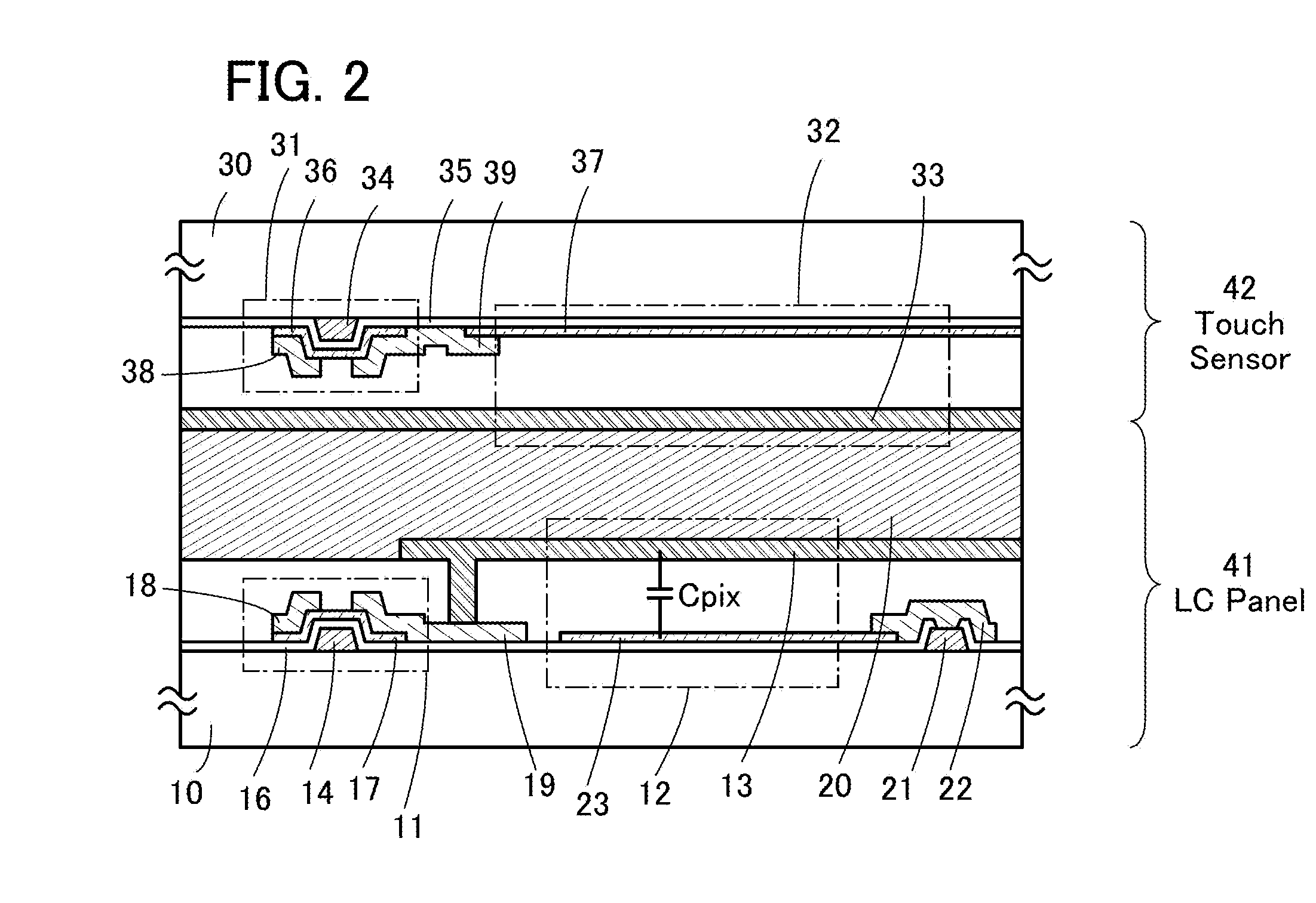
[0097]In this embodiment, a modification example of the display device in Embodiment 1 is described.

[0098]FIG. 2 shows a modification example of the cross-sectional schematic view described using FIG. 1A.

[0099]In FIG. 1A, the Cpix includes the conductive layer 15 and the conductive layer 19; however, another structure may be used. For example, a structure shown in FIG. 2 can be used.

[0100]In FIG. 2, an electrode 23 connected to a conductive layer 21 through a conductive layer 22 is used as one electrode of the Cpix.

[0101]The conductive layer 21 is formed in the same layer as the conductive layer 14. The conductive layer 22 is formed in the same layer as the conductive layers 18 and 19. The electrode 23 is formed in the same layer as the semiconductor layer 17.

[0102]Furthermore, in the case where the transistor 11 is an OS transistor, the electrode 23 provided in the same layer as the semiconductor layer 17 can be formed using the same material as the semiconductor layer 17. In this ...

embodiment 3

[0140]In this embodiment, a cross-sectional view of the display device described in Embodiments 1 and 2 is described in detail.

[0141]FIG. 10 is a cross-sectional schematic view of the display device of one embodiment of the present invention. In the display device illustrated in FIG. 10, a touch sensor and a liquid crystal element are provided between a pair of substrates, so that the display device can be thin.

[0142]FIG. 10 is a cross-sectional view of terminal portions 250a and 250b, a driver circuit portion 250d, and a pixel portion 250p which are included in the display device. In the pixel portion 250p, pixels of three colors of red (R), green (G), and blue (B) express one color. Note that in the cross-sectional view illustrated here, a pixel Pr of red (R) and a pixel Pg of green (G) are shown in the pixel portion 250p, and a pixel of blue (B) is not shown. The pixel Pr of red (R) includes a liquid crystal element 201r, and the pixel Pg of green (G) includes a liquid crystal el...


PUM

PropertyMeasurementUnit
angleaaaaaaaaaa
angleaaaaaaaaaa
angleaaaaaaaaaa

Abstract

To provide a display device with a novel structure that can achieve both thickness reduction and favorable display quality. In a structure of a display device including a liquid crystal layer between a pixel electrode and a counter electrode, a common electrode and an electrode of a capacitor in a touch sensor on the counter electrode side are formed integrally and supplied with a pulse signal. On the element substrate side, a signal to be supplied to a capacitor line that forms a capacitance with the pixel electrode is in conjunction with the pulse signal so as to cancel a change in an electric field applied to the liquid crystal layer. Such a structure can achieve a display device with a touch sensor function that can cancel a change in an electric field applied to a liquid crystal layer even when the electric field is changed by a pulse signal.

Description

BACKGROUND OF THE INVENTION[0001]1. Field of the Invention[0002]One embodiment of the present invention relates to a display device, a display module, and an electronic device.[0003]Note that one embodiment of the present invention is not limited to the above technical field. The technical field of the invention disclosed in this specification and the like relates to an object, a method, or a manufacturing method. In addition, one embodiment of the present invention relates to a process, a machine, manufacture, or a composition of matter. Specifically, examples of the technical field of one embodiment of the present invention disclosed in this specification include a semiconductor device, a display device, a light-emitting device, a power storage device, a memory device, a method for driving any of them, and a method for manufacturing any of them.[0004]2. Description of the Related Art[0005]Display devices with a touch sensor function are widely used (see Patent Document 1).REFERENC...

Claims


Application Information

Patent Timeline
Patent Type & Authority Applications(United States)
IPC IPC(8): G02F1/1362G02F1/1343G02F1/1368H01L27/12H01L29/786
CPCG02F1/136286H01L27/1225H01L29/7869H01L27/1255G02F1/134309G02F1/1368G02F1/136277G02F1/136213H01L27/124G02F1/13338G02F1/136G06F3/0412G06F3/04184G06F3/0445G09G3/3655G09G2300/0809G06F3/041
Inventor MIYAKE, HIROYUKIKUSUNOKI, KOJIISHITANI, TETSUJIHATSUMI, RYO
Owner SEMICON ENERGY LAB CO LTD
Why Eureka
Try Eureka