

Light emitting device
a technology of light-emitting devices and light-emitting components, which is applied in the direction of semiconductor devices, basic electric elements, electrical appliances, etc., can solve the problems of significant reduction in thermal resistance and deterioration of reliability of light-emitting devices, and achieve the effect of minimizing the occurrence of voids during soldering
- Summary
- Abstract
- Description
- Claims
- Application Information
AI Technical Summary
Benefits of technology
Problems solved by technology
Method used
Image

Examples
Embodiment Construction
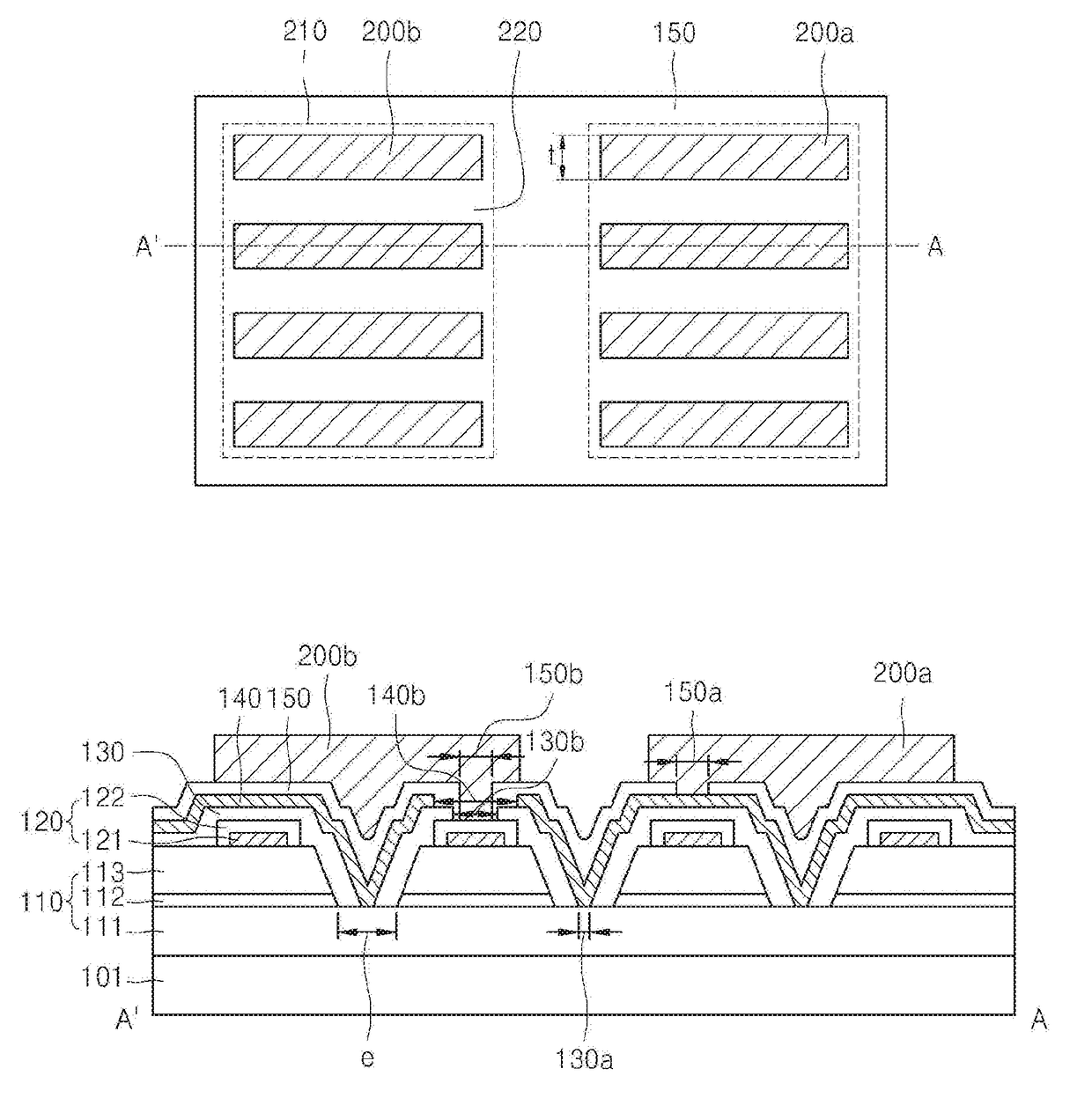
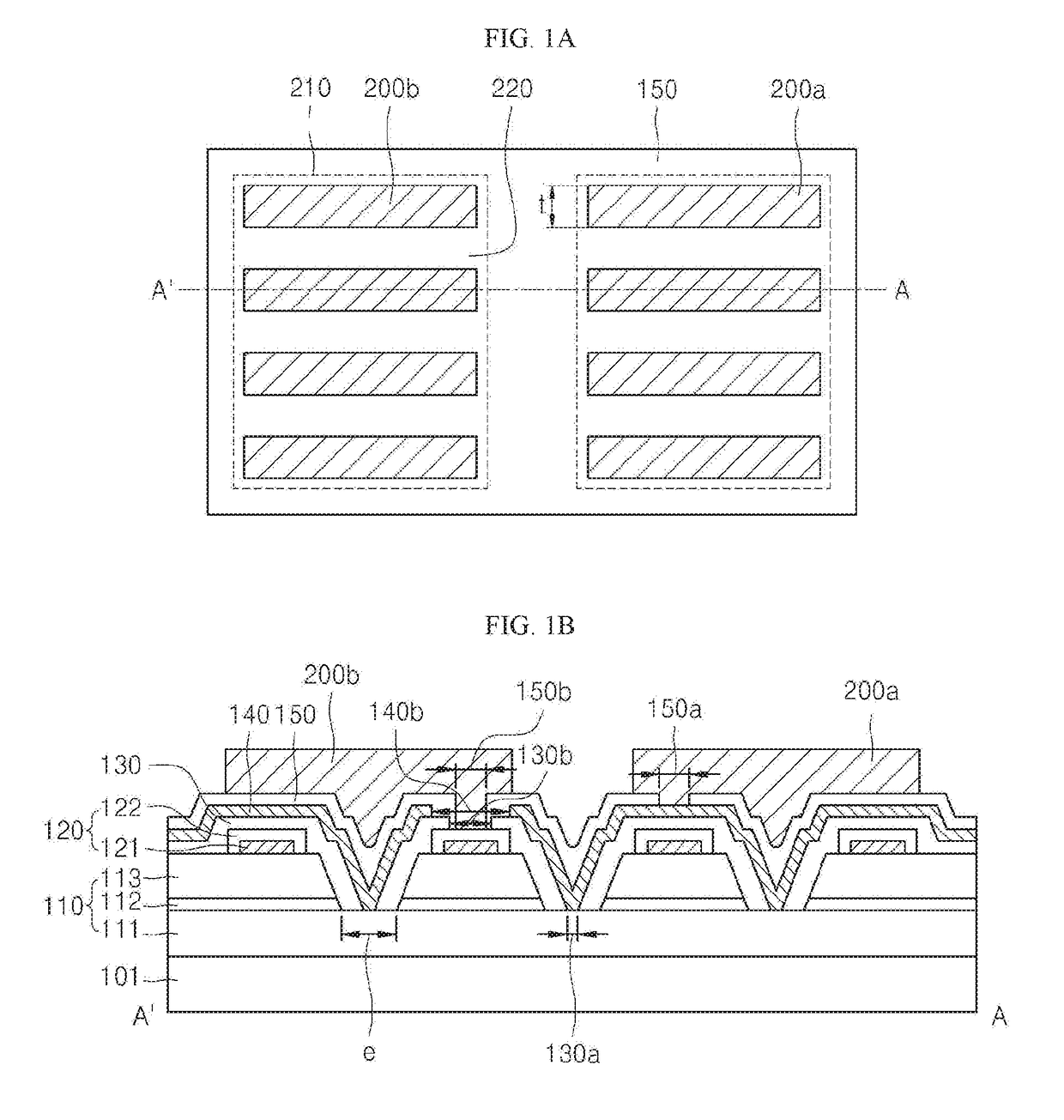
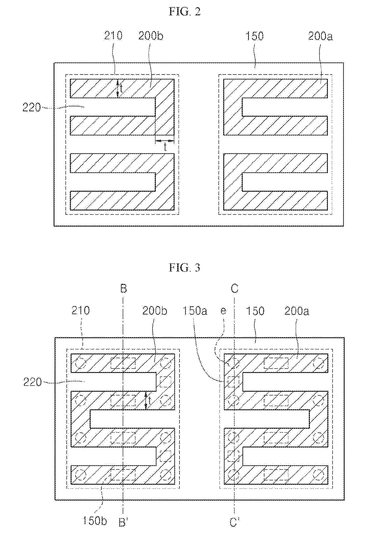
[0078]In the following description, for the purposes of explanation, numerous specific details are set forth in order to provide a thorough understanding of various exemplary embodiments. It is apparent, however, that various exemplary embodiments may be practiced without these specific details or with one or more equivalent arrangements. In other instances, well-known structures and devices are shown in block diagram form in order to avoid unnecessarily obscuring various exemplary embodiments.
[0079]Unless otherwise specified, the illustrated exemplary embodiments are to be understood as providing exemplary features of varying detail of various exemplary embodiments. Therefore, unless otherwise specified, the features, components, modules, layers, films, panels, regions, and / or aspects of the various illustrations may be otherwise combined, separated, interchanged, and / or rearranged without departing from the disclosed exemplary embodiments. Further, in the accompanying figures, the...
PUM
 Abstract
Description
Claims
Application Information