This helps you quickly interpret patents by identifying the three key elements:
Problems solved by technology
Method used
Benefits of technology
Benefits of technology
The patent describes a new structure for electronic devices that allows the front face to display more images without the need for a black matrix. This structure also improves the efficiency of mounting components in the device.
Problems solved by technology
Therefore, a component mounting structure related to a display may be insufficient in the mounting space of a display driverintegrated circuit (DDIC), a fingerprint sensor, or a pressure sensor, and there may be a restriction particularly in utilizing a display region.
Further, in the structure in which the display mounting structure implements the front face of the electronic device as a full display, there may be a limit in reducing the black matrix (BM) region.
Method used
Image
Click on the blue label to locate the original text in one second.
Reading with bidirectional positioning of images and text.
Examples
Embodiment Construction
[0060]The following description with reference to the accompanying drawings is provided to assist in a comprehensive understanding of various embodiments of the disclosure as defined by the claims and their equivalents. It includes various specific details to assist in that understanding but these are to be regarded as merely exemplary. Accordingly, those of ordinary skill in the art will recognize that various changes and modifications of the various embodiments described herein can be made without departing from the scope and spirit of the disclosure. In addition, descriptions of well-known functions and constructions may be omitted for clarity and conciseness.
[0061]The terms and words used in the following description and claims are not limited to the bibliographical meanings, but, are merely used by the inventor to enable a clear and consistent understanding of the disclosure. Accordingly, it should be apparent to those skilled in the art that the following description of variou...
PUM
Abstract
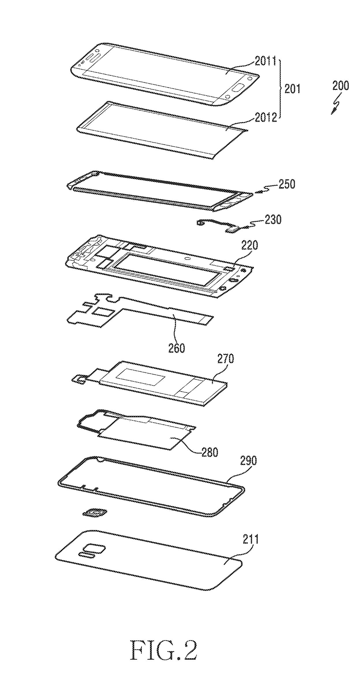
An electronic device for widening an active area of a display is provided. The electronic device includes a housing including a first plate and a second plate facing away from the first plate, a touch screen display including a first glass plate, a second glass plate, and an organic light-emitting diode (OLED) layer interposed between the first plate and the second plate, a flexible layer including a first portion connected to the first surface of the second glass plate and bent around an edge of the second glass plate toward the second plate of the housing, and a second portion extending from the first portion and interposed between the second glass plate and the second plate of the housing, a display driverintegrated circuit (DDIC) mounted on a first surface of the second portion of the flexible layer, and a printed circuit board (PCB) including a portion mounted on a second surface of the second portion of the flexible layer.
Description
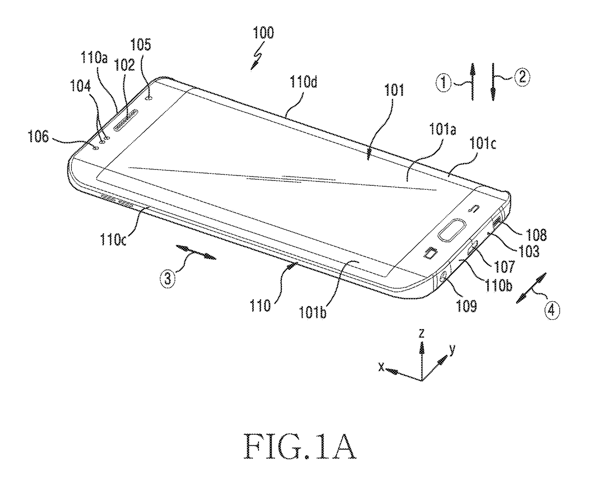
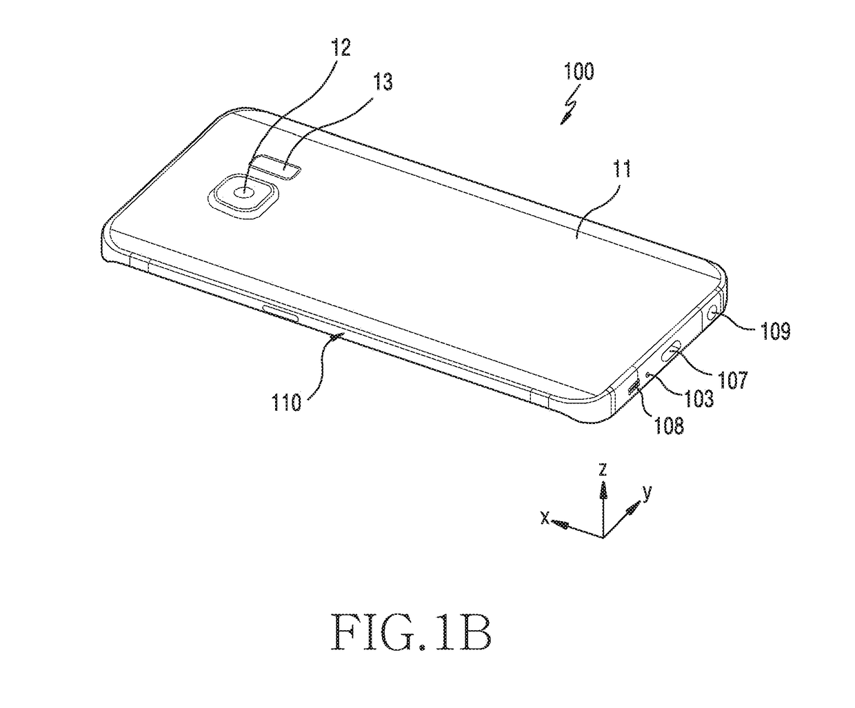
CROSS-REFERENCE TO RELATED APPLICATION(S)[0001]This application is based on and claims priority under 35 U.S.C. § 119(a) of a Korean patent application number 10-2017-0085876, filed on Jul. 6, 2017, in the Korean Intellectual Property Office, the disclosure of which is incorporated by reference herein in its entirety.BACKGROUND1. Field[0002]The disclosure relates to an electronic device including a display.2. Description of Related Art[0003]An ordinary electronic device has a display (e.g., a touch-screen display) disposed on a front face thereof, and efforts are being made to increase the proportion occupied by an active area where a screen is displayed in the entire display area on the disposed display.[0004]Further, the electronic device may include a fingerprint sensor or a pressure sensor, and the display region and the fingerprint sensor region may be distinguished from each other.[0005]The above information is presented as background information only to assist with an underst...
Claims
Application Information
Patent Timeline
Application Date:The date an application was filed.
Publication Date:The date a patent or application was officially published.
First Publication Date:The earliest publication date of a patent with the same application number.
Issue Date:Publication date of the patent grant document.
PCT Entry Date:The Entry date of PCT National Phase.
Estimated Expiry Date:The statutory expiry date of a patent right according to the Patent Law, and it is the longest term of protection that the patent right can achieve without the termination of the patent right due to other reasons(Term extension factor has been taken into account ).
Invalid Date:Actual expiry date is based on effective date or publication date of legal transaction data of invalid patent.

