Method for gettering an image display apparatus

a technology for display apparatus and image, which is applied in the direction of vacuum obtaining/maintenance, discharge tube luminescnet screen, electric discharge tube/lamp manufacture, etc., can solve the problems of damage to the apparatus, failure to display a bright image, and failure to meet the requirements of the application

Inactive Publication Date: 2003-11-25
CANON KK
View PDF27 Cites 15 Cited by
  • Summary
  • Abstract
  • Description
  • Claims
  • Application Information

AI Technical Summary

Benefits of technology

Another object of the present invention is to provide an image display apparatus with little change of the luminance over time, and a method for producing the same.
Still another object of the present invention is to provide an image display apparatus with little generation of unevenness in the image display area over time, and a method for producing the same.

Problems solved by technology

If the pressure in the vacuum chamber is elevated by gas generated therein, such gas detrimentally influences the electron source to lower the amount of electron emission, thereby disabling the display of a bright image, though the level of such influence depends on the kind of the gas.
Also, such generated gas is ionized by the electron beam, and the generated ions are accelerated by the electric field and may collide with the electron source, causing damage thereto.
A discharge may also be generated in the vacuum chamber, eventually leading to the destruction of the apparatus.
However, in the recently developed flat panel display utilizing the electron source consisting of a plurality of electron emitting elements provided on a flat substrate, a specific drawback is that the gas generated from the image displaying member reaches the electron source before reaching the getter, thereby inducing a local increase of the pressure and deterioration of the electron source resulting therefrom.
However, in the above-described image display apparatus, although the deterioration of the electron source caused by the gas generated in the vacuum chamber can be prevented to a certain extent by positioning a larger number of getter members in the vacuum chamber, it is difficult to efficiently absorb such generated gas.
This difficulty results in the deterioration of the electron source over time or unevenness in the luminance of the displayed image, unless certain particular consideration is given to the positioning of such getter members.

Method used


Image

  • Method for gettering an image display apparatus
  • Method for gettering an image display apparatus
  • Method for gettering an image display apparatus

Examples


first embodiment

In this reference example, an image display apparatus was prepared in the same manner as in the first embodiment, except that an evaporating getter was positioned on only one side outside the image display area.

In this reference example, the evaporating getter 14 was provided on one side outside the image display area as shown in FIGS. 20A and 20B, and the getter film was formed by flushing the evaporating getter 14 with a heating wire 15 after sealing.

Each of the image display apparatuses of the foregoing embodiments first to fifth and the reference example was subjected to simple matrix drive to effect continuous light emission over the entire surface and the luminance variation in time was measured.

As a result, though there was a difference in the initial luminance, the image display apparatus of the first to fifth embodiments showed little decrease of the luminance and little fluctuation in the luminance among the pixels even after a prolonged drive, in comparison with the appar...

sixth embodiment

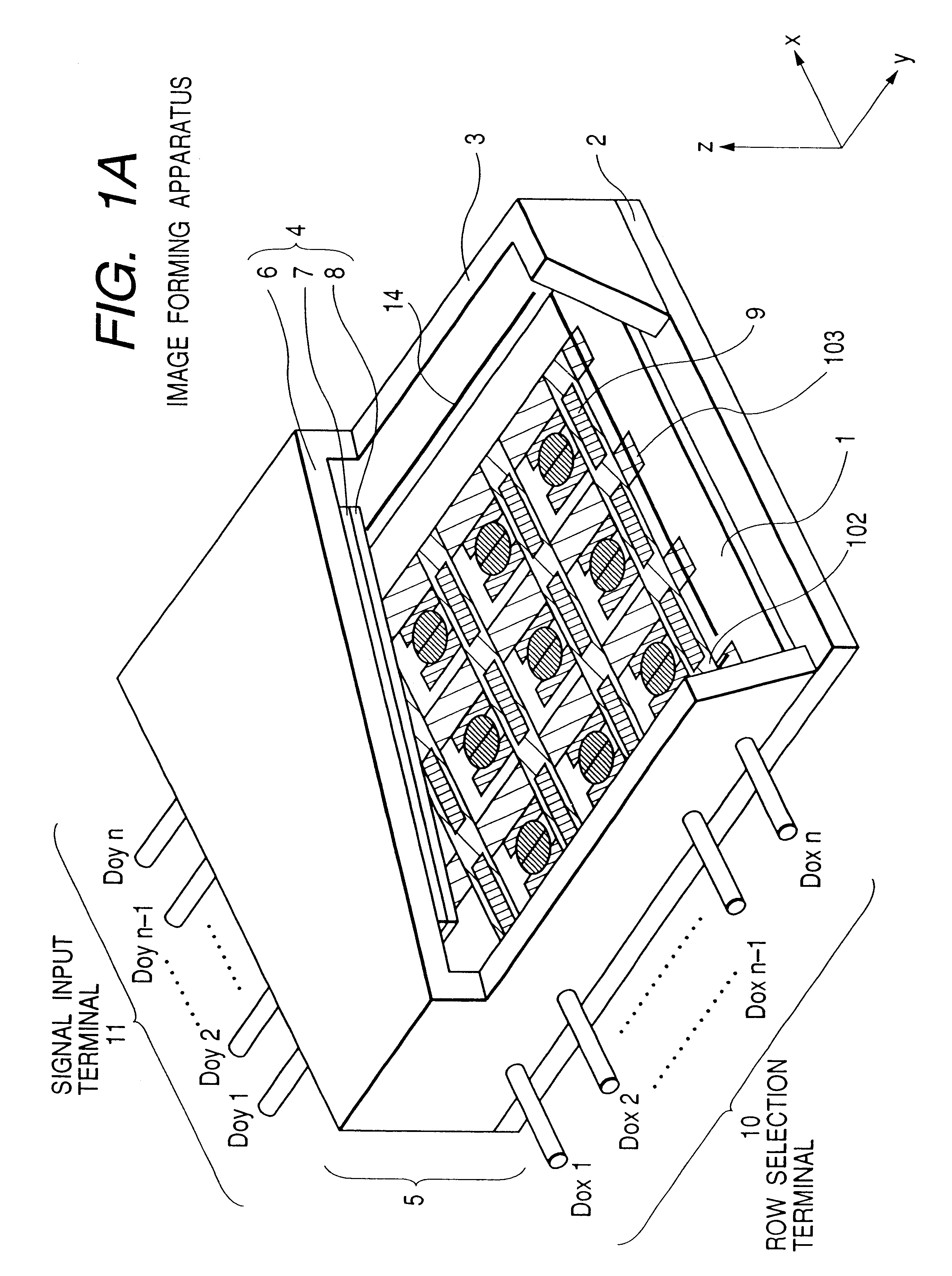
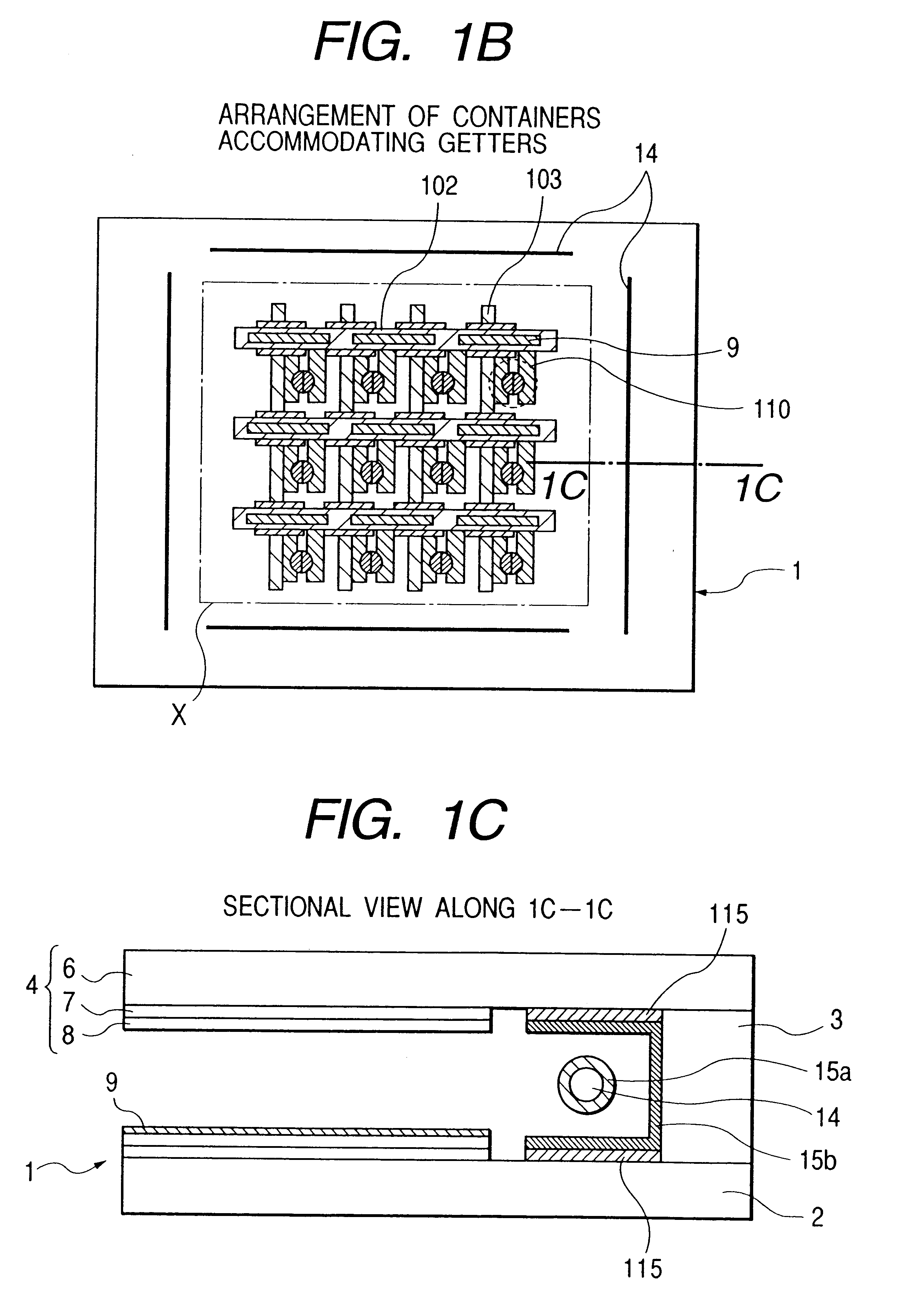
The image display apparatus of this embodiment is similar in configuration to that shown in FIGS. 5A to 5C, wherein the non-evaporating getters 9 are provided on substantially the entire surface of the row wirings (upper wirings) 102 in the image display area and the non-evaporating getters 14 are provided on the insulation layer 115 covering the column wirings (lower wirings) 103 outside the image display area on the electron source substrate 1.

The image display apparatus of the present embodiment is provided, on the substrate 1, with an electron source consisting of plural surface conduction electron emitting elements wired in a simple matrix structure (100 rows.times.100 columns).

FIG. 21 is a partial plan view of the electron source substrate 1, while FIGS. 22A and 22B are cross-sectional views along lines 22A--22A and 22B--22B in FIG. 21, respectively. The same components are represented by the same numbers in FIGS. 21, 22A and 22B. There are shown an electron source substrate 1...

seventh embodiment

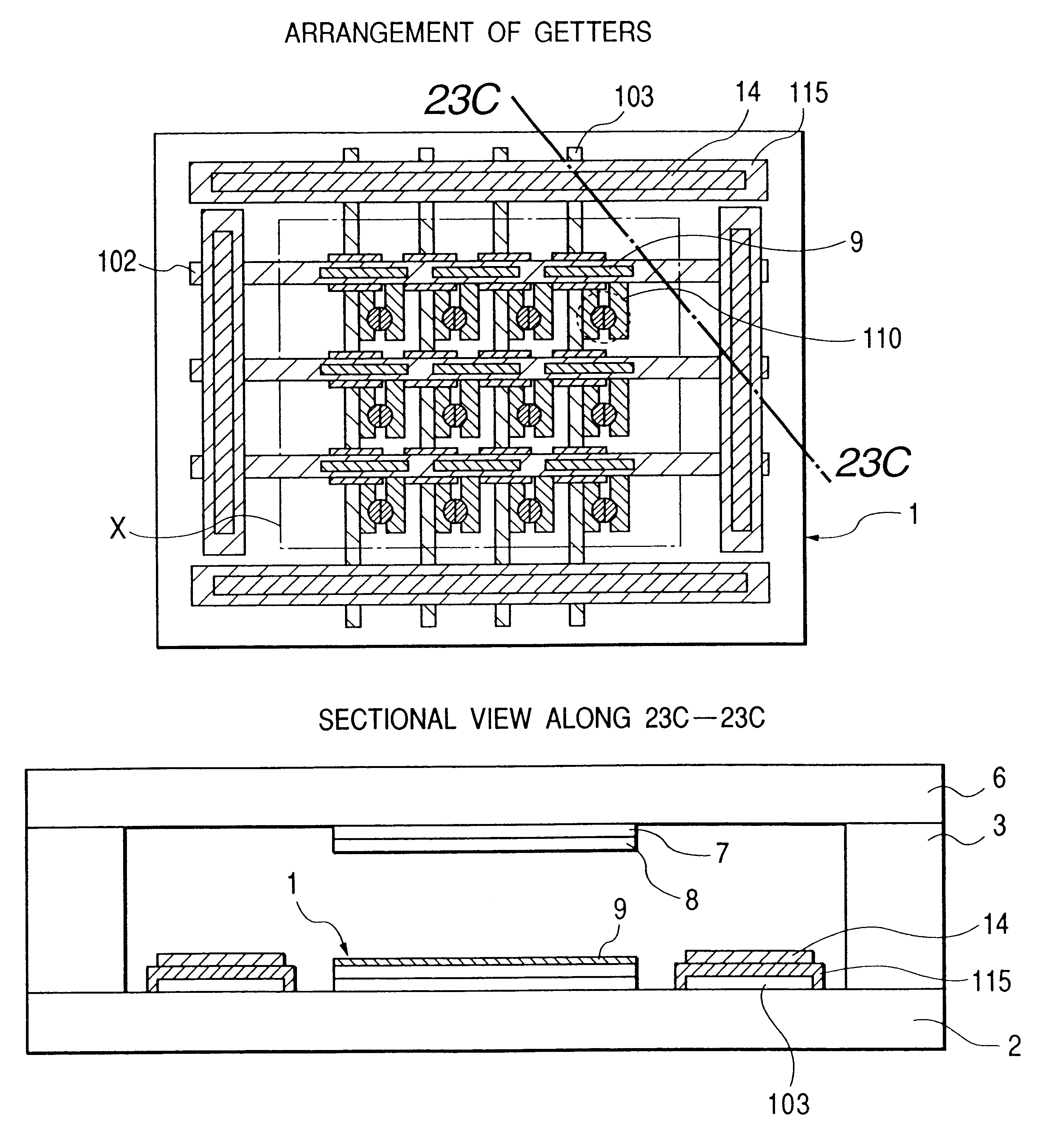
FIGS. 23A to 23C show the image display apparatus of this embodiment.

In the present embodiment, the following step f-2 was executed between the steps f and g in the foregoing sixth embodiment.

Step f-2

The insulation film 115, consisting of a silicon oxide film of a thickness of 1.0 .mu.m, was deposited by RF sputtering also on the upper wirings 102 outside the image display area.

Also, in step x of the foregoing sixth embodiment, in forming the getters on the upper wirings 102 in the image display area and the lower wirings 103 outside the image display area, the getter layers 9, 14 consisting of a Ar--V--Fe alloy were formed by also sputtering on the insulation film 115 of the upper wirings 102 outside the image display area. The thickness of the getter layers 9, 14 was adjusted to 2 .mu.m. The sputtering target used had a composition of Zr 70%, V 25 % and Fe 5% (ratio by weight).

Steps other than those mentioned above were executed in the same manner as in the foregoing sixth embodim...


PUM


Abstract

An image display apparatus is provided with an external housing constituted by members including first and second substrates positioned with a gap therebetween, an electron source positioned on the first substrate in the external housing, and a fluorescent film and an accelerating electrode provided on the second substrate. A first getter is positioned in the image display area in the external housing. A second getter is provided, so that it is insulated from the electron source and the accelerating electrode, which surrounds the first getter.

Description

1. Field of the InventionThe present invention relates to an image display apparatus provided with an electron source, and a method for producing the same.2. Related Background ArtIn an apparatus for displaying an image by irradiating a fluorescent member, which is an image displaying member, with an electron beam from an electron source to cause the fluorescent member to emit light, it is necessary to maintain the interior of a vacuum chamber, containing the electron beam and the image displaying member, at a high vacuum. If the pressure in the vacuum chamber is elevated by gas generated therein, such gas detrimentally influences the electron source to lower the amount of electron emission, thereby disabling the display of a bright image, though the level of such influence depends on the kind of the gas. Also, such generated gas is ionized by the electron beam, and the generated ions are accelerated by the electric field and may collide with the electron source, causing damage ther...

Claims


Application Information

Patent Timeline
Patent Type & Authority Patents(United States)
IPC IPC(8): H01J29/94H01J29/00H01J9/385H01J9/38
CPCH01J9/385H01J29/94H01J2329/00H01J2201/3165
Inventor HASEGAWA, MITSUTOSHIGOFUKU, IHACHIROHAMAMOTO, YASUHIROSHIGEOKA, KAZUYAARAI, YUTAKA
Owner CANON KK
Why Eureka
Try Eureka