Surface shape recognition sensor and method of manufacturing the same

Inactive Publication Date: 2005-01-18
NIPPON TELEGRAPH & TELEPHONE CORP
View PDF20 Cites 14 Cited by
  • Summary
  • Abstract
  • Description
  • Claims
  • Application Information

AI Technical Summary

Benefits of technology

It is, therefore, the main object of the present invention to suppress a deterioration in cleanliness on the detection surface of a surface shape recognition sensor such as a fingerprint sensor used for, for example, authentication due to residues such as fingerprint residues le

Problems solved by technology

Furthermore, fingerprint residues interfere as noise with authentication, and hence degrade the authentication performance of the f

Method used


Image

  • Surface shape recognition sensor and method of manufacturing the same
  • Surface shape recognition sensor and method of manufacturing the same
  • Surface shape recognition sensor and method of manufacturing the same

Examples


Example

[First Embodiment]

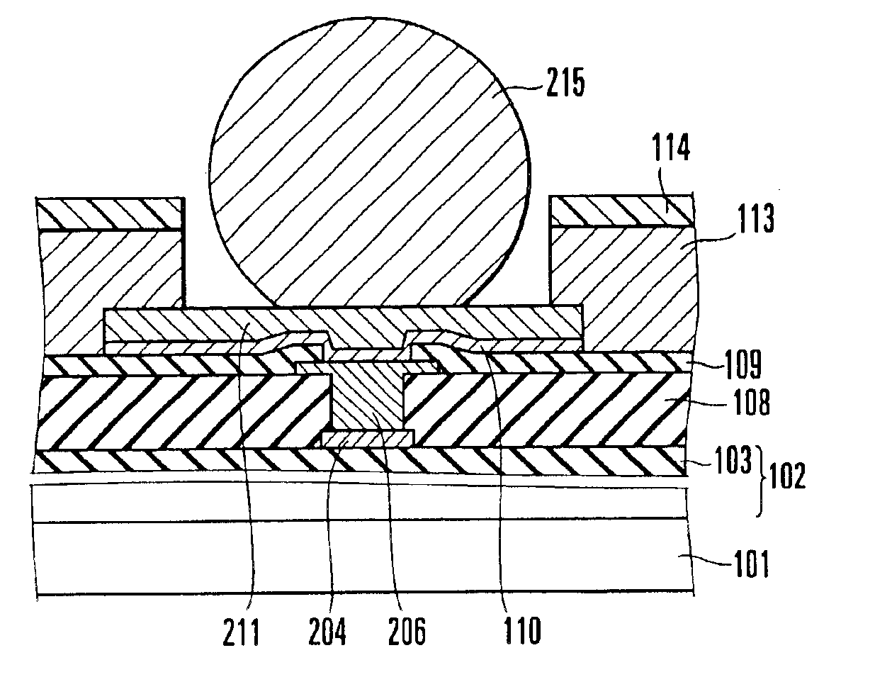
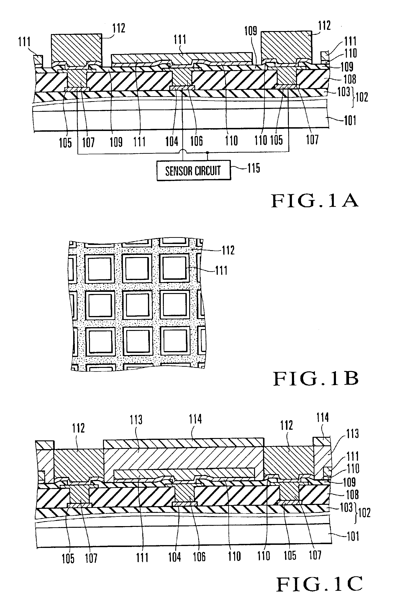
The first embodiment of the present invention will be described first. FIGS. 1A, 1B, and 1C explain a method of manufacturing a surface shape recognition sensor (sensor chip) according to this embodiment. The state shown in FIG. 1A will be described first. First of all, a multilevel interconnection layer 102 is formed on a semiconductor substrate 101 made of, for example, silicon. The uppermost layer of the multilevel interconnection layer 102 is covered with an insulating film 103, and interconnections 104 and 105 are formed on the insulating film 103.

The multilevel interconnection layer 102 is formed from a plurality of elements such as MOS transistors (not shown) and a plurality of interconnections (not shown) which connect the elements, and forms a sensor circuit 115 and the like. The interconnections 104 and 105 are connected to these circuits. Note that an illustration of the sensor circuit 115 is omitted in subsequent drawings, e.g., FIGS. 1C, 3, and 4.

The i...

Example

[Second Embodiment]

Another embodiment of the present invention will be described next.

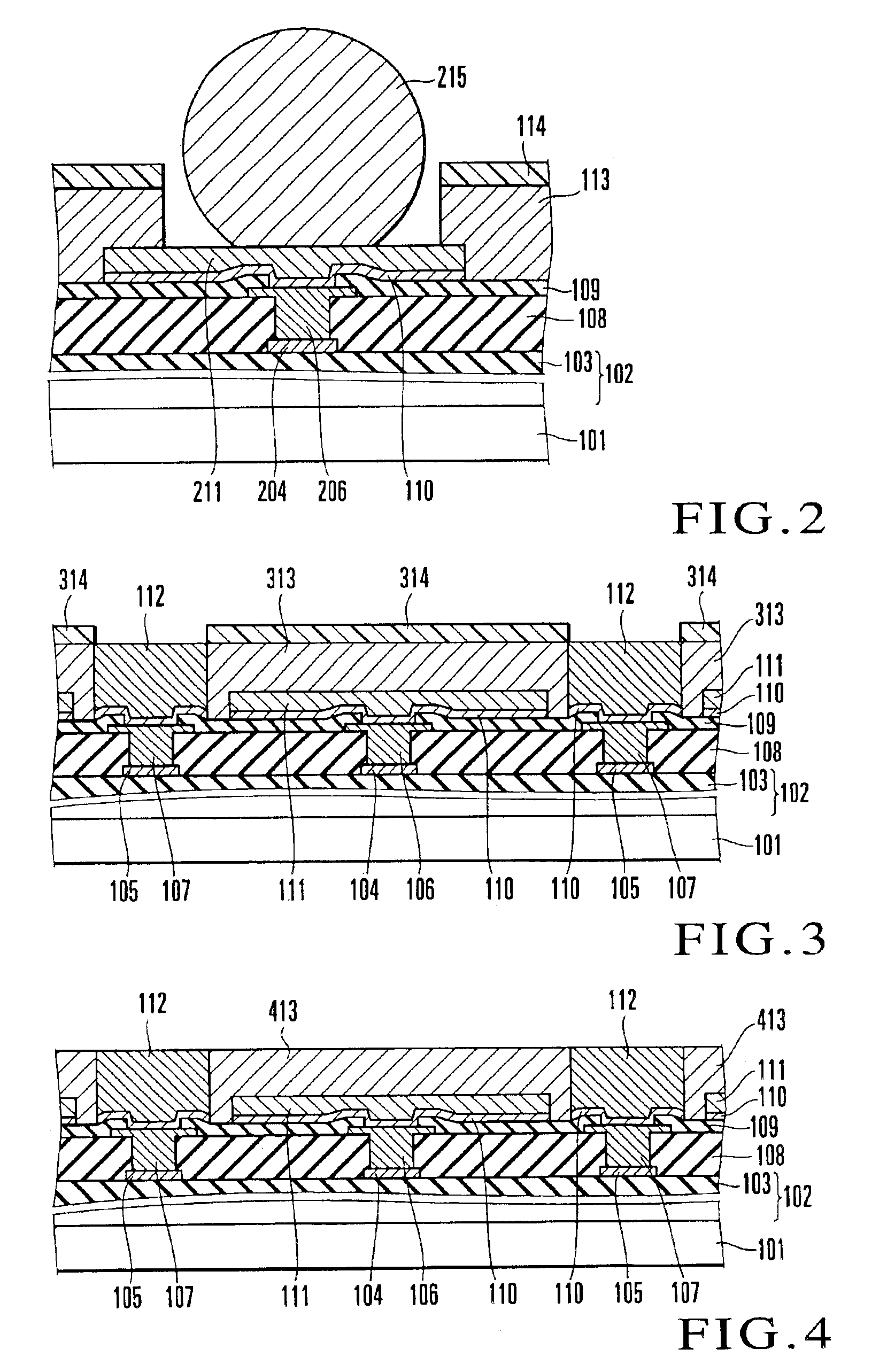
FIG. 3 schematically shows the structure of a surface shape recognition sensor according to this embodiment.

In the surface shape recognition sensor shown in FIG. 3, an insulating protective film 313 serving as a capacitance film formed on a sensor electrode 111 is made of silicon nitride, and a surface protective film 314 is made of polybenzoxazole. The insulating protective film 313 and surface protective film 314 in FIG. 3 are identical to those in FIG. 1C, and hence a description thereof will be omitted.

Assume that residues such as fingerprint residues left on the detection surface of the surface shape recognition sensor which a detection target touches are sebum. In this embodiment, since a polybenzoxazole film absorbs sebum, almost no fingerprint residues are left on the surface protective film 314. Polybenzoxazole also has a hydrophobic property (water repellency) so water-soluble foreign sub...

Example

[Third Embodiment]

As described above, a fluoroplastic film made of a fluorocarbon material can also be formed on the surface of a surface shape recognition sensor having no ground electrode. Even in a surface shape recognition sensor having no ground electrode as shown in FIG. 5B, a bump 610 serving as an external connection terminal is formed on an outer peripheral portion of the sensor chip, as shown in FIG. 6. In this case as well, as described above, if a surface protective film made of a fluorocarbon material, i.e., a fluoroplastic film, is formed by coating the chip with a coating solution in which a fluorocarbon material that forms a film having a hydrophobic property is dissolved, the formation of a surface protective film on the external connection terminal (bump 610) is suppressed.

This mechanism will be described in more detail below.

As shown in FIG. 5A, in a surface shape recognition sensor, a multilevel interconnection layer 502 is formed on a semiconductor substrate 501...


PUM


Abstract

A surface shape recognition sensor of this invention has a surface protective film having a hydrophobic property on an insulating protective film which is made of an insulator and formed to cover a sensor electrode, and includes at least a ground electrode which is formed on the substrate such that the ground electrode is partly exposed on the surfaces of the insulating protective film and surface protective film so as to be insulated/isolated from the sensor electrode and come into contact with the surface of a detection target. This sensor prevents fingerprint residues from easily remaining and improves tamper resistance.

Description

BACKGROUND OF THE INVENTIONThe present invention relates to a surface shape recognition sensor used to sense a surface shape having fine recesses and projections such as human fingerprints and animal's noseprints and a method of manufacturing the sensor and, more particularly, to a surface shape recognition sensor whose recognition surface is protected and a method of manufacturing the sensor.With the recent proliferation of the Internet, a great deal of attention has been paid to the importance of authentication. Biometrics, in which authentication is performed by measuring / evaluating biological characteristics, has greatly advanced as a technical field of authentication. Authentication using fingerprints, in particular, has been vigorously studied as an authentication means for measuring / evaluating a physical characteristic that cannot be easily changed. In order to perform authentication by using a fingerprint, the fingerprint is read. Systems for reading fingerprints include var...

Claims


Application Information

Patent Timeline
IPC IPC(8): A61B5/117G06K9/00G01B7/28G06T1/00
CPCG06K9/0002A61B5/1172G06V40/1306
Inventor ISHII, HIROMUYAGI, SHOUJIMACHIDA, KATSUYUKIKYURAGI, HAKARU
Owner NIPPON TELEGRAPH & TELEPHONE CORP
Why Eureka
Try Eureka