PZT (111) texture through Ir texture improvement

a ferroelectric dielectric layer and texture technology, applied in the field of integrated circuit processing, can solve the problems of difficult formation of such a textured pzt ferroelectric dielectric layer, personal devices requiring more computational power and on-chip memory, and reducing the rough microstructure of the bottom electrode diffusion barrier layer, so as to eliminate any microstructure roughness

a ferroelectric dielectric layer and texture technology, applied in the field of integrated circuit processing, can solve the problems of difficult formation of such a textured pzt ferroelectric dielectric layer, personal devices requiring more computational power and on-chip memory, and reducing the rough microstructure of the bottom electrode diffusion barrier layer, so as to eliminate any microstructure roughness

US6872669B1Active Publication Date: 2005-03-29TEXAS INSTR INC

Image

  • PZT (111) texture through Ir texture improvement
  • PZT (111) texture through Ir texture improvement
  • PZT (111) texture through Ir texture improvement

Examples


Embodiment Construction

pect of the present invention;

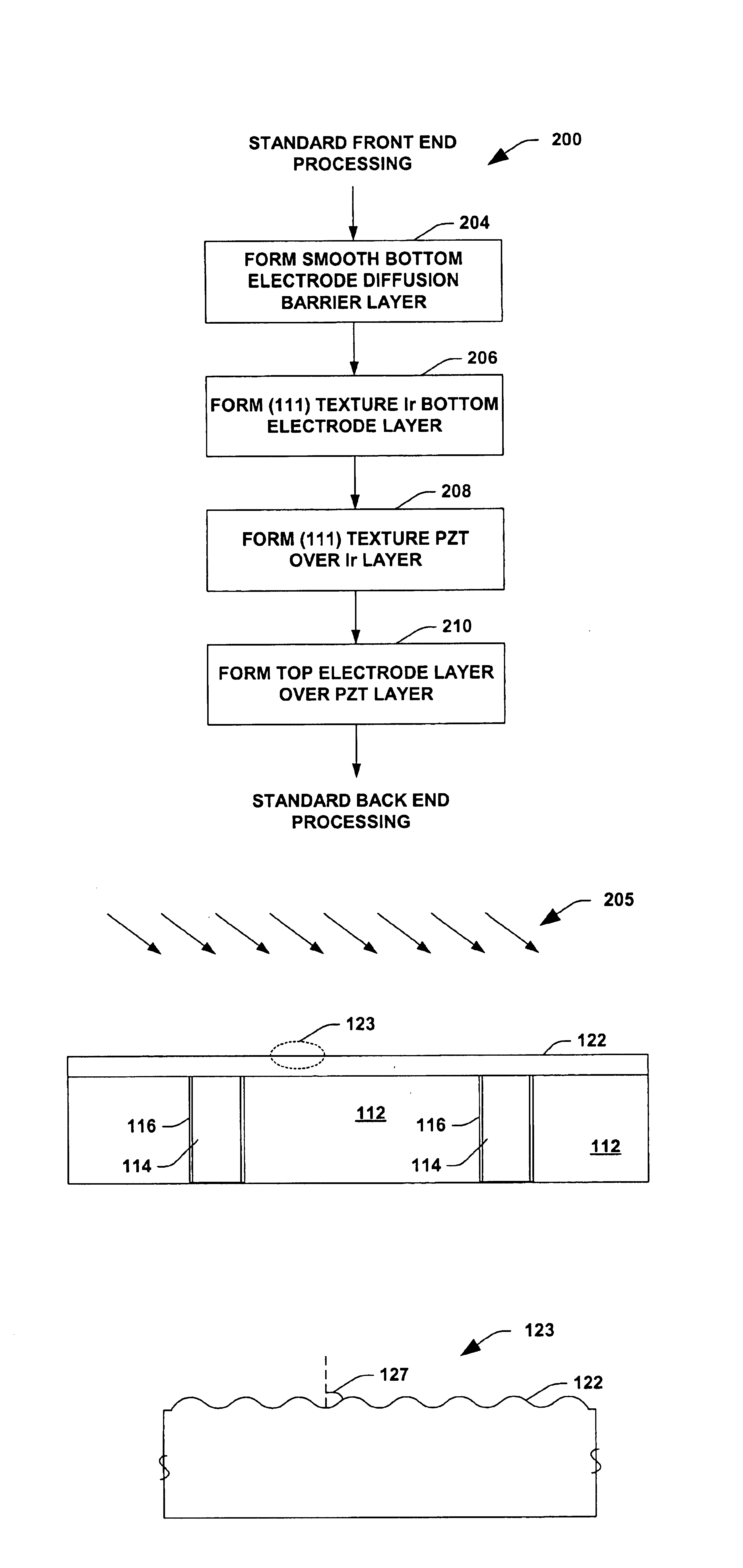
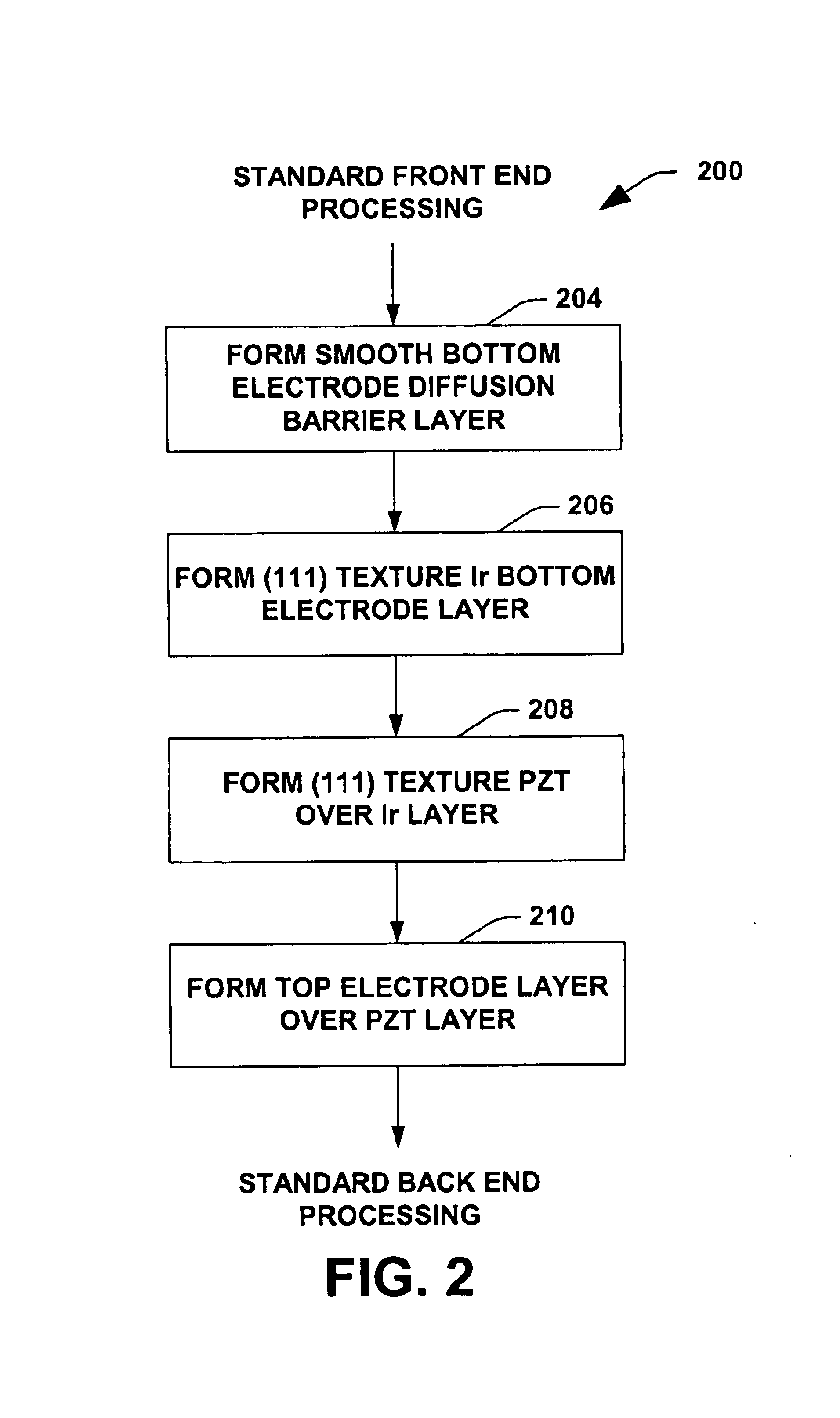
[0022]FIG. 6 is an exploded fragmentary cross section of a surface portion of the bottom electrode diffusion barrier layer having a smooth upper surface due to the ion beam smoothing of FIG. 5; and

[0023]FIGS. 7A and 7B are side elevation and plan views, respectively, of an exemplary CMP apparatus for employment in planarizing a bottom electrode diffusion barrier layer in accordance with another aspect of the invention.

DETAILED DESCRIPTION OF THE INVENTION

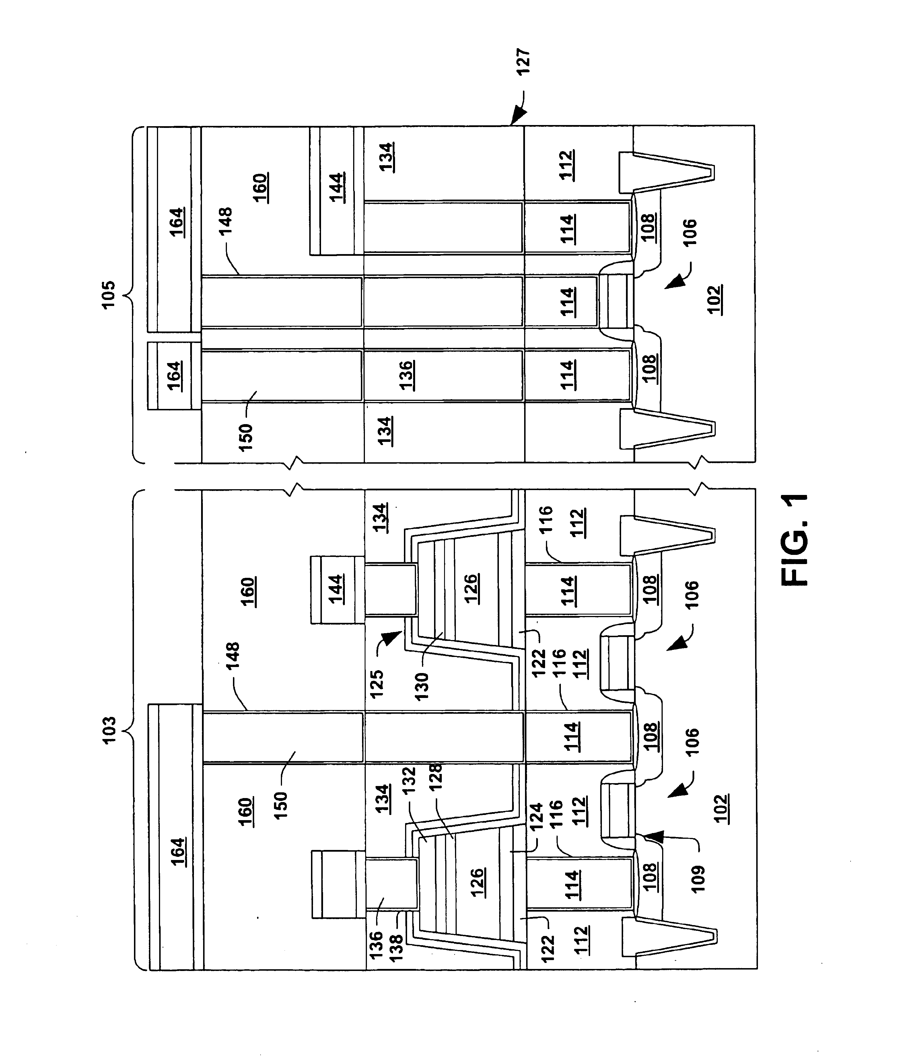
[0024]The present invention will now be described with respect to the accompanying drawings in which like numbered elements represent like parts. The figures provided herewith and the accompanying description of the figures is merely provided for illustrative purposes. One of ordinary skill in the art should realize, based on the instant description, other implementations and methods for fabricating the devices and structures illustrated in the figures and in the following description. The present inven...


PUM

PropertyMeasurementUnit
surface microstructure angleaaaaaaaaaa
microstructure angleaaaaaaaaaa

Abstract

The present invention is directed to a method of forming a ferroelectric capacitor having a (111) PZT texture. The method includes forming a smooth bottom electrode diffusion barrier layer that facilitates a preferential (111) texture in the subsequently formed bottom electrode layer. The (111) bottom electrode layer texture than facilitates a high quality (111) texture in the overlying PZT layer, thereby improving bit-to-bit polarization charge uniformity for various capacitors as the ferroelectric capacitor sizes continue to shrink.

Description

FIELD OF THE INVENTION[0002]The present invention relates generally to the field of integrated circuit processing, and more particularly relates to an FeRAM structure and a method of manufacture thereof having a PZT ferroelectric dielectric layer having a generally (111) texture.BACKGROUND OF THE INVENTION[0003]Several trends exist, today, in the semiconductor device fabrication industry and the electronics industry. Devices are continuously getting smaller and smaller and requiring less and less power. A reason for this is that more personal devices are being fabricated which are very small and portable, thereby relying on a small battery as its supply source. For example, cellular phones, personal computing devices, and personal sound systems are devices in great demand in the consumer market. In addition to being smaller and more portable, personal devices are requiring more computational power and on-chip memory. In light of all these trends, there is a need in the industry to p...

Claims


Application Information

Patent Timeline
29 Mar 2005
Publication
US6872669B1
IPC
H01L21/02; H01L21/302; H01L21/314; H01L21/316; H01L21/321; H01L21/3213
CPC
H01L21/3145; H01L21/31691; H01L28/55; H01L21/3212; H01L28/75; H01L28/65; H01L21/32131; H01L21/02197
Inventors
SUMMERFELT, SCOTT R.; AGGARWAL, SANJEEV