Complex band-pass DeltaSigma AD modulator for use in AD converter circuit

a ad modulator and deltasigma technology, applied in the field of complex bandpass ad modulators, can solve the problems of difficult to realize a ad modulator of a higher precision, the precision of the entire ad converter is deteriorated, and methods can only be applied to a real band-pass ad modulator having a single input terminal and a single output terminal, so as to achieve a simple configuration and reduce power consumption and chip area

Inactive Publication Date: 2006-08-29
SEMICON TECH ACADEMIC RES CENT
View PDF21 Cites 18 Cited by
  • Summary
  • Abstract
  • Description
  • Claims
  • Application Information

AI Technical Summary

Benefits of technology

[0076]An essential object of the present invention is therefore to provide a complex band-pass ΔΣ AD modulator having a simpler configuration and achieving a higher speed as compared with those of the prior art.
[0087]According to the complex band-pass ΔΣ AD modulator of the present invention, there can be provided the complex band-pass ΔΣ AD converter circuit and the digital radio receiver using the same having a simpler configuration and executing a process at a speed higher than that of the prior art. More concretely, the DWA algorithm capable of applying a first-order noise shaping to a non-linearity of the DA converter of the multi-bit complex band-pass ΔΣ AD modulator for processing first and second signals orthogonal to each other can be realized by means of hardware circuit by additionally supplying a relatively small-size digital circuit and an analog multiplexer to the hardware circuit. Accordingly, reductions in power consumption and chip area can be realized in, for example, Bluetooth and a Low-IF receiver of broad-band LAN or the like.

Problems solved by technology

However, in contrast to the one-bit DA converter having a superior linearity, it is not possible for a non-linearity of an internal DA converter of a multi-bit ΔΣ AD modulator to be noise-shaped on the inside of the modulator, and this leads to disadvantageous deterioration in the precision of the entire AD converter.
It is clearly understood from the Equation (3) that the quantization noise E (z) of the internal AD converter AD1 is noise-shaped, however, the non-linearity error δ (z) of the DA converter DA1 is not noise-shaped and directly outputted, and this leads to that it is difficult to realize a ΔΣ AD converter of a higher precision.
However, those methods can only be applied to a real band-pass ΔΣ AD modulator having a single input terminal and a single output terminal, as shown in FIGS. 2A and 2B.
However, it is actually impossible to realize such a circuit.
For example, when the signal C1 (n) is always a positive integer of 2, the input signal C2 (n) inputted to the DA converter DA2 is infinite according to increase of a timing “n” and eventually exceeds an input range of the DA converter DA2, and this leads to that it impossible to accurately realize the DA conversion.
If it was possible to replace the multi-bit DA converter on the inside of the high-pass ΔΣ AD modulator by the circuit shown in FIGS. 7A and 7B, the non-linearity of the DA converter could be noise-shaped, however, such a circuit cannot be realized in a manner similar to that of the low-pass ΔΣ AD modulator.
It is understood from the Equation (2) that the quantization noise E (z) of the internal AD converter is noise-shaped, however, the non-linearity error δ(z) of the DA converter DA3 is not subjected to the noise shaping and directly outputted, and this leads to that it is difficult to realize the ΔΣ AD converter achieving a higher precision.
More concretely, the DA converter of multi-bit type includes the non-linearity resulting from a matching precision generated in the device, which adversely affects the performance of the entire AD converter circuit.
In particular, there is caused an even more serious problem when a refining process is adopted in order to downsize and accelerate the circuit.
Although the AD converter circuit using the complex band-pass ΔΣ modulator was proposed in the first to fourth patent documents, the proposed AD converter circuit can not solve any mentioned problems.

Method used


Image

  • Complex band-pass DeltaSigma AD modulator for use in AD converter circuit
  • Complex band-pass DeltaSigma AD modulator for use in AD converter circuit
  • Complex band-pass DeltaSigma AD modulator for use in AD converter circuit

Examples


Embodiment Construction

[0119]Preferred embodiments according to the present invention will be described below with reference to the attached drawings. In the description below, components similar to each other are denoted by the same numerical references.

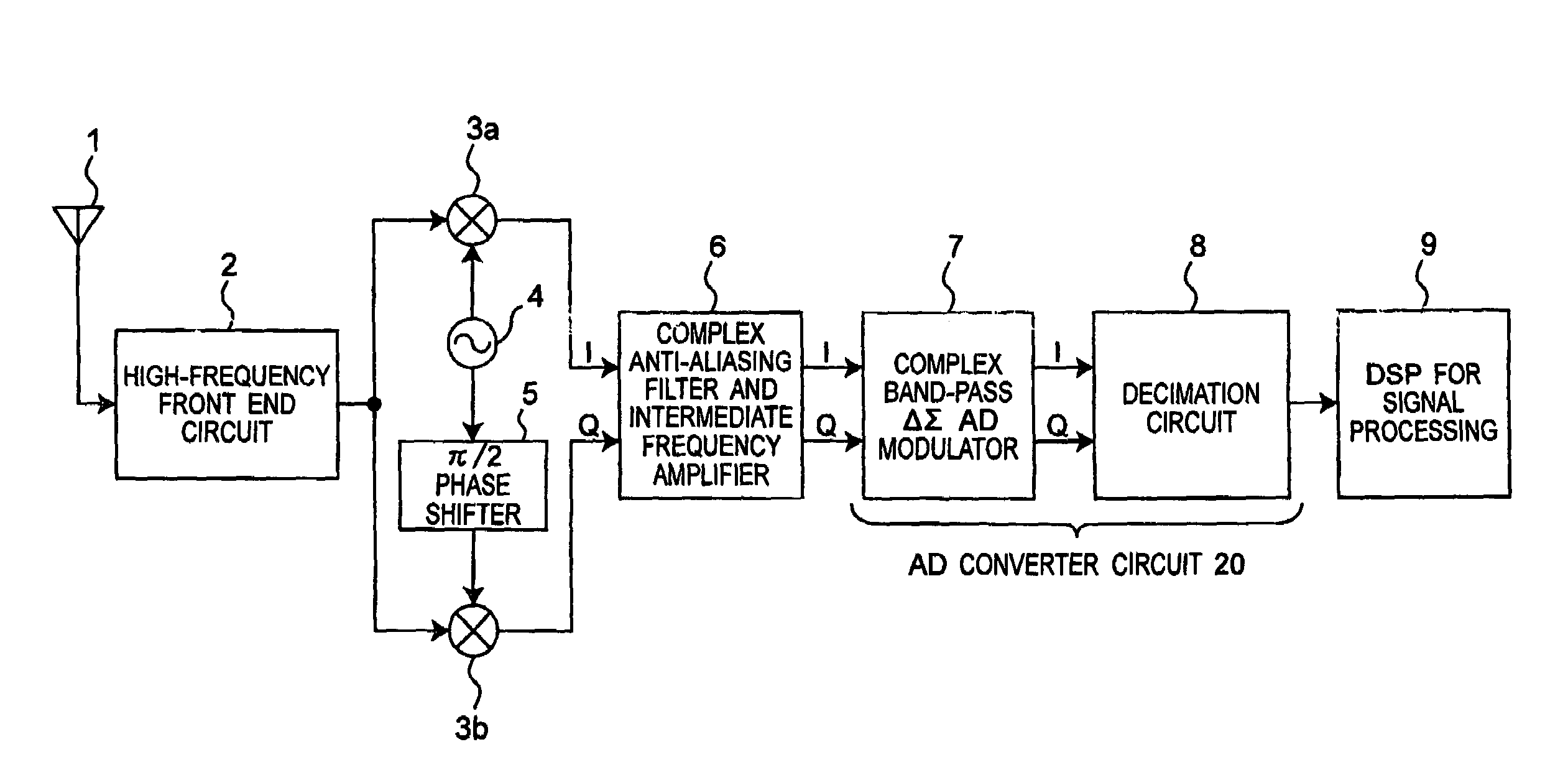
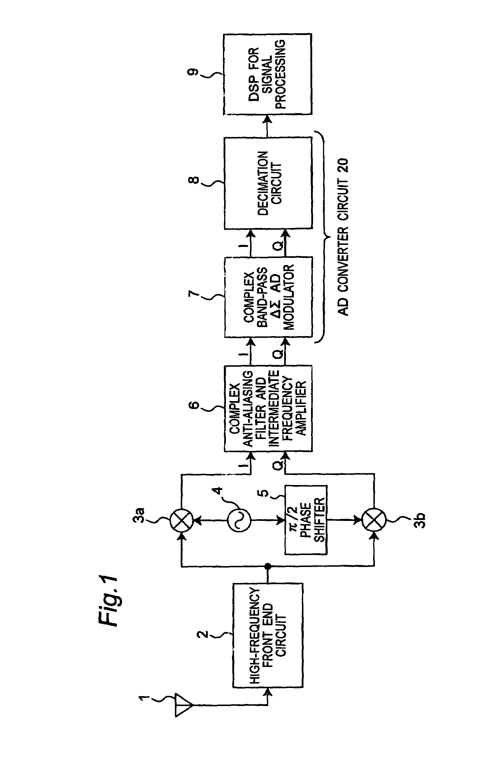
[0120]FIG. 1 is a block diagram showing a configuration of a digital radio receiver having an AD converter circuit 20 including a complex band-pass ΔΣ AD modulator 7, and a decimation circuit 8, according to a preferred embodiment of the present invention. A digital radio receiver according to the present embodiment is characterized by including a complex band-pass ΔΣ AD modulator 7 of FIG. 15 as described later. In particular, in the present embodiment, in order to realize the complex band-pass ΔΣ AD modulator achieving a higher precision using an algorithm capable of noise-shaping non-linearities of internal multi-bit DA converters DA11 and DA12 of the complex band-pass ΔΣ AD modulator 7 in which an I signal and a Q signal are used as input and output s...


PUM


Abstract

A complex band-pass ΔΣ AD modulator is provided with a subtracter device, a complex band-pass filter, first and second AD converters, and first and second DA converters. The first and second DA converters and first and second logic circuits are sandwiched by first and second multiplexers. At a first timing of a clock signal, the first multiplexer inputs and outputs the first and second digital signals as they are, and at a second timing thereof, the first multiplexer inputs the first and second digital signals, and outputs the first digital signal as a second digital signal and outputs the second digital signal as a first digital signal. The second multiplexer inputs and outputs first and second analog signals similarly. The first and second logic circuits substantially noise-shapes non-linearities of the first and second DA converters by realizing complex digital and analog filters, using high-pass and low-pass element rotation methods.

Description

BACKGROUND OF THE INVENTION[0001]1. Field of the Invention[0002]The present invention relates to a complex band-pass ΔΣ AD modulator, an AD converter circuit, and a digital radio receiver, and in particular, to a complex band-pass ΔΣ AD modulator for use in a digital radio receiver or the like, an AD converter circuit using the complex band-pass ΔΣ AD modulator, and a digital radio receiver using the AD converter circuit.[0003]2. Description of the Related Art[0004]Application of a band pass ΔΣ AD converter to an RF receiver circuit in a communication system such as a mobile phone and a radio LAN has been under consideration (for example, See first to fifth non-patent documents). Further, in an application used in the communication system (in particular, Low-IF receiver), the application of a complex band-pass ΔΣ AD modulator capable of suppressing an image signal generated on the inside of the modulator due to a mismatch between I path and Q path has been also under consideration s...

Claims


Application Information

Patent Timeline
Patent Type & Authority Patents(United States)
IPC IPC(8): H03M3/00H03M1/00H04B14/06H03M1/06H03M3/04
CPCH03M3/34H03M1/0665H03M3/464H03M3/424H03M3/40
Inventor SAN, HAOKOBAYASHI, HARUOWADA, HIROKIWADA, ATSUSHI
Owner SEMICON TECH ACADEMIC RES CENT
Why Eureka
Try Eureka