

Semiconductor memory device, controller, and read/write control method thereof
a semiconductor memory and controller technology, applied in the direction of memory adressing/allocation/relocation, digital storage, instruments, etc., can solve the problems of increasing the cost of the controller lsi, increasing the complexity of the internal process, and insufficient actualization of the mounting number of nonvolatile memories to be comprised in the memory card, so as to reduce the cost of the controller and the semiconductor memory devi
- Summary
- Abstract
- Description
- Claims
- Application Information
AI Technical Summary
Benefits of technology
Problems solved by technology
Method used
Image



Examples
Embodiment Construction
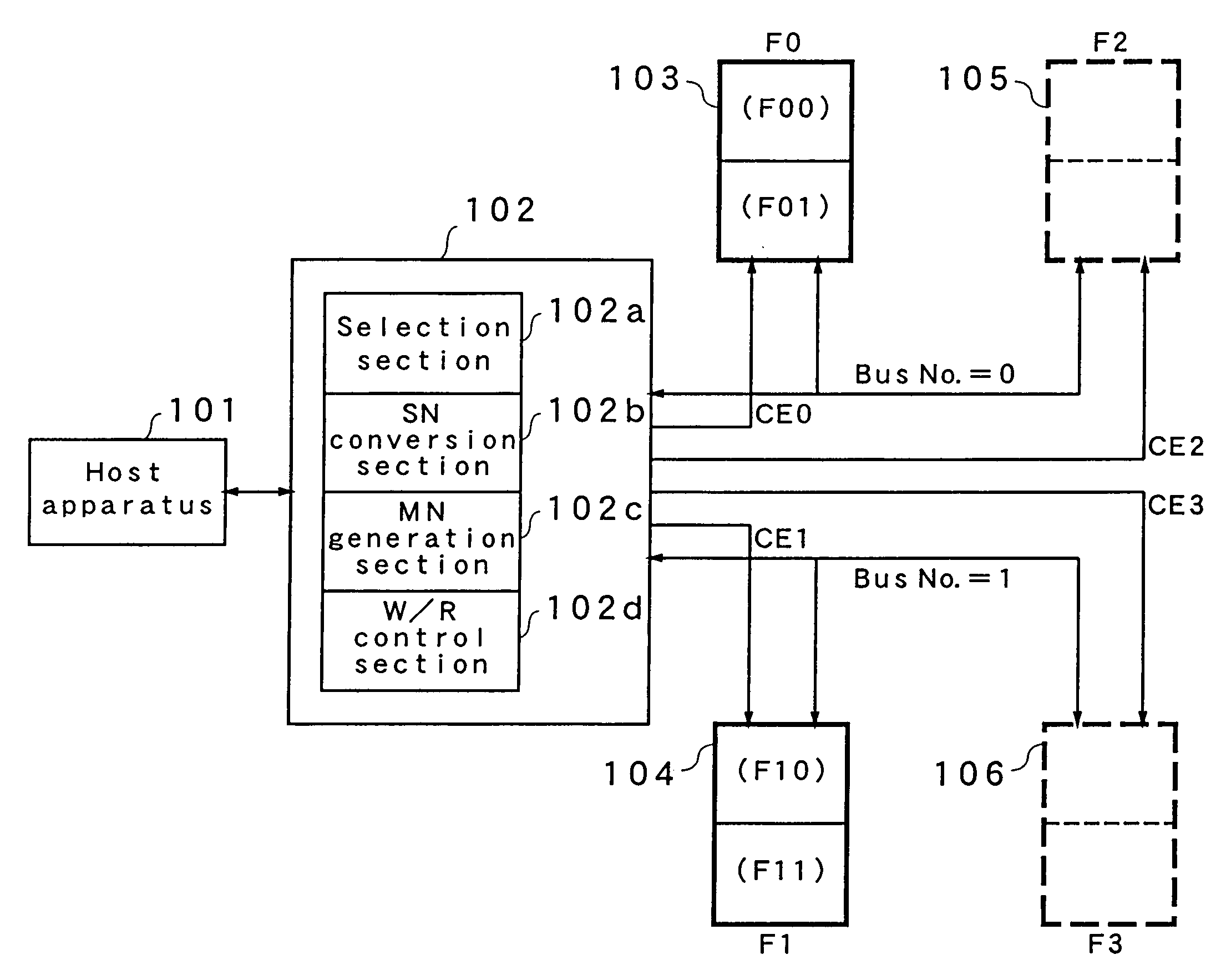
[0015]A semiconductor memory device and a controller thereof according to an embodiment of the present invention will now be described using the drawings. FIG. 1 is a block diagram showing a configuration of the semiconductor memory device according to this embodiment. The semiconductor memory device includes a controller 102 and a plurality of flash memories 103 to 106. Herein, each of the flash memories 103, 104, 105, 106 are sometimes referred to as F0, F1, F2, F3.
[0016]The controller 102 converts a logical address into a physical address with respect to a consecutive logical address column transferred in accordance with a data write command or a read command from a host apparatus 101 and performs a data write operation or a data read operation for the four flash memories 103, 104, 105, 106 or the two flash memories 103, 104. Herein, the flash memories 105, 106 are shown with a broken line, indicating that they can be omitted when the nonvolatile memory is a two-flash memory conf...
PUM
 Abstract
Description
Claims
Application Information