Supercharge Your Innovation With Domain-Expert AI Agents!

Flash memory device and program method

a flash memory and program technology, applied in the field of flash memory devices, can solve the problems of reducing the width of the line, affecting neighboring cells sharing the same word line, and reducing the area efficiency of the program, and achieve the effect of increasing the area efficiency

Inactive Publication Date: 2010-03-23
SK HYNIX INC
View PDF5 Cites 8 Cited by
  • Summary
  • Abstract
  • Description
  • Claims
  • Application Information

AI Technical Summary

Benefits of technology

[0009]One embodiment of the present invention is directed to a method to reduce the interference between neighboring cells by performing a program operation on all cells sharing the same word line (i.e., programming on a word line basis).
[0010]The other embodiment of the present invention is directed to increasing area efficiency by sharing the page buffer between two cell strings when programming is performed on a word line basis.

Problems solved by technology

However, as the level of integration of a flash memory device increases, the line width decreases and the gap between memory cells becomes close.
Thus, neighboring cells sharing the same word line are interfered by the voltage of the programmed cell.
However, the interference phenomenon between memory cells becomes more profound in the MLC.
This is because cells of a programmed even page are interfered by cells of an odd page that are programmed next.
Accordingly, the reliability of devices may be significantly degraded.

Method used


Image

  • Flash memory device and program method
  • Flash memory device and program method
  • Flash memory device and program method

Examples


first embodiment

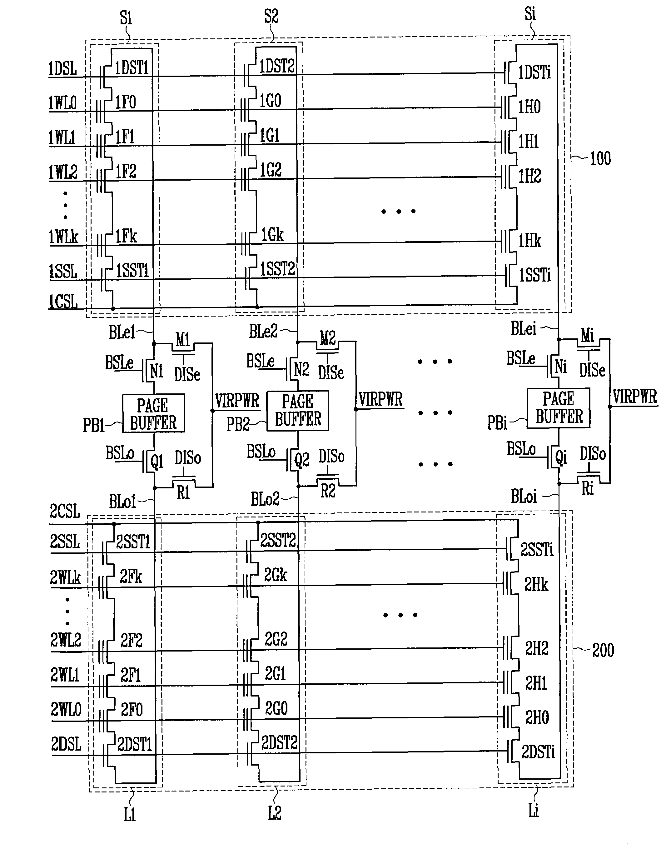
[0027]FIG. 3A is a block diagram of a flash memory device according to the present invention.

[0028]Referring to FIG. 3A, the flash memory device includes a memory cell array 100 having a plurality of cell strings S1 to Si (i is an integer). Each of the plurality of cell strings S1 to Si includes a plurality of memory cells (not shown) for storing data. The plurality of cell strings S1 to Si are connected to a plurality of page buffers PB1 to PBi, respectively, through bit lines BL1 to BLi. That is, one cell string corresponds to one page buffer. Accordingly, the page buffer and the cell string perform a program operation on a word line basis in a corresponding manner one by one. This is described below in detail with reference to FIG. 3B.

[0029]FIG. 3B is a detailed circuit diagram of FIG. 3A.

[0030]The memory cell array 100 includes the plurality of cell strings S1 to Si. The cell strings S1 includes a drain select transistor DST1, a source select transistor SST1 and a plurality of m...

second embodiment

[0033]FIG. 4A is a block diagram of the flash memory device according to the present invention. According to the embodiment of FIG. 3B, the interference phenomenon between the memory cells is reduced, but the area is increased since each cell string requires its own page buffer. Thus, a memory cell array sharing the plurality of page buffers may be further included in order to increase the area efficiency.

[0034]The plurality of page buffers PB1 to PBi form pairs with two memory cell arrays 100 and 200. The memory cell array 100 includes a plurality of cell strings S1 to Si. The memory cell array 200 includes a plurality of cell strings L1 to Li. Page buffers PB1 to PBi are disposed between the cell strings S1 to Si and the cell strings L1 to Li so that the cell strings S1 to Si and the cell strings L1 to Li are symmetrical to each other. Each of the cell arrays S1 to Si share a page buffer PB1 to PBi with each of the cell arrays L1 to Li as can be seen in FIG. 4A. That is, since two...


PUM


Abstract

A method for programming a flash memory device includes selecting bit lines connected to a plurality of memory strings and selecting a word line. A lower bit is programmed into the memory cells connected to the selected word line and programming a upper bit into the memory cells. The step of selecting the word line and the step of programming the upper bit are repeated.

Description

CROSS-REFERENCE TO RELATED APPLICATIONS[0001]This application claims priority from Korean Patent Application No. 2006-96099, filed on Sep. 29, 2006, the contents of which are incorporated herein by reference in its entirety.BACKGROUND OF THE INVENTION[0002]The present invention relates to a flash memory device and, more particularly, to a programming method, in which an interference phenomenon between memory cells can be prevented.[0003]FIG. 1 is a block diagram of a conventional flash memory device.[0004]Referring to FIG. 1, the flash memory device includes a memory cell array 10 and page buffers P1 to Pn (n is an integer). The memory cell array 10 includes a plurality of cell strings Cle to Cne and Clo to Cno. Each of the plurality of cell strings Cle to Cne and Clo to Cno includes a plurality of memory cells (not shown) for storing data. The page buffers P1 to Pn are connected to the plurality of cell strings Cle to Cne and Clo to Cno through an even bit line BLe and an odd bit l...

Claims


Application Information

Patent Timeline
Patent Type & Authority Patents(United States)
IPC IPC(8): G11C16/04
CPCG11C16/0483G11C16/10G11C16/3418G11C16/3427G11C11/5628G11C16/08G11C16/24
Inventor KIM, KI SEOG
Owner SK HYNIX INC
Features
  • R&D
  • Intellectual Property
  • Life Sciences
  • Materials
  • Tech Scout
  • Unparalleled Data Quality
  • Higher Quality Content
  • 60% Fewer Hallucinations
Learn More