Display device and electronic apparatus

a display device and electronic equipment technology, applied in the direction of static indicating devices, instruments, etc., can solve the problems of reducing affecting the yield of the product, and changing the luminance of the light-emitting element el over time, so as to reduce the manufacturing cost and reduce the frame size of the panel

Active Publication Date: 2012-03-20
JOLED INC
View PDF12 Cites 6 Cited by
  • Summary
  • Abstract
  • Description
  • Claims
  • Application Information

AI Technical Summary

Benefits of technology

[0017]According to the mode of the present invention, the control terminal (gate) of the switching transistor is connected to the scan line disposed on a row previous to that of the scan line connected to the control terminal (gate) of the sampling transistor. Corresponding to this configuration, the scanner of the drive part line-sequentially drives the sampling transistors and the switching transistors included in the respective pixels by sequentially supplying the control signal to the scan lines along the rows. In other words, the sampling transistors and the switching transistors included in the respective pixels are line-sequentially driven by one scanner. By thus reducing the number of scanners included in the drive part to the minimum value, the manufacturing cost is reduced. Furthermore, for a structure in which the peripheral drive part is formed integrally with the pixel array part on the same panel, reduction in the frame size of the panel can be achieved and thus the yield can be enhanced because the layout area of the drive part can be decreased.

Problems solved by technology

Therefore, if the characteristic of the light-emitting element EL changes over time, the potential of the source S is affected and thus Vgs changes, which leads to aging change in the drain current Ids supplied from the drive transistor T2.
This results in a problem that the luminance of the light-emitting element EL changes over time.
This leads to variation in the light-emission luminance from pixel to pixel, which is a problem that should be solved.
However, the pixel with such correction functions has a complex circuit configuration, and a switching transistor is desired in addition to the drive transistor and the sampling transistor.
However, the addition of the scanner to the drive part leads to a problem of causing increase in the product cost.
Furthermore, a structure in which the peripheral drive part is formed integrally with the pixel array part on the same panel involves a problem that the addition of the scanner causes the lowering of the panel yield.
Moreover, the addition of the scanner inevitably causes increase in the layout area of the peripheral drive part.
The increase in the layout area of the peripheral drive part inevitably causes enlargement of the frame part of the panel and thus leads to the lowering of the yield, which is a problem that should be solved.

Method used


Image

  • Display device and electronic apparatus
  • Display device and electronic apparatus
  • Display device and electronic apparatus

Examples


Embodiment Construction

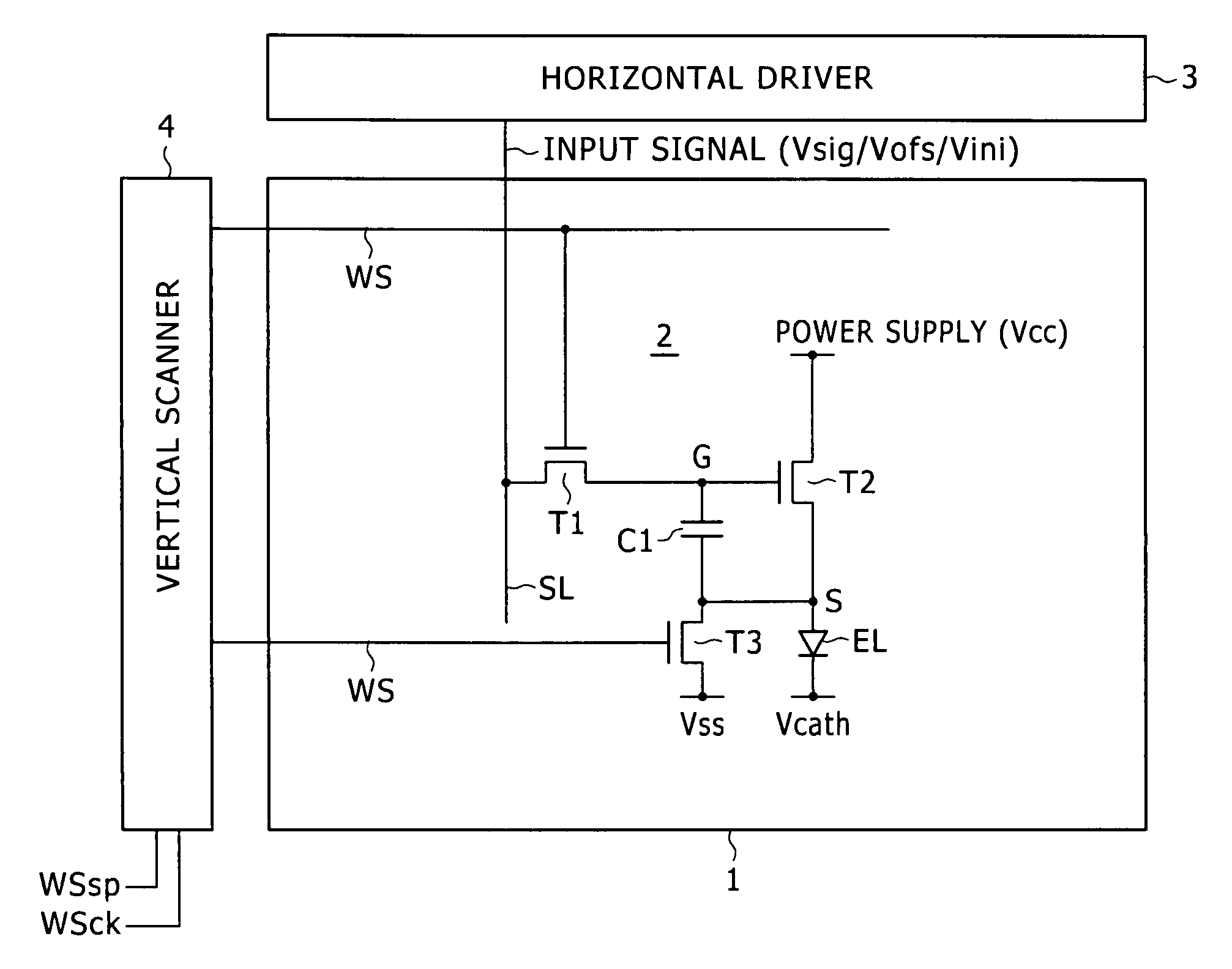
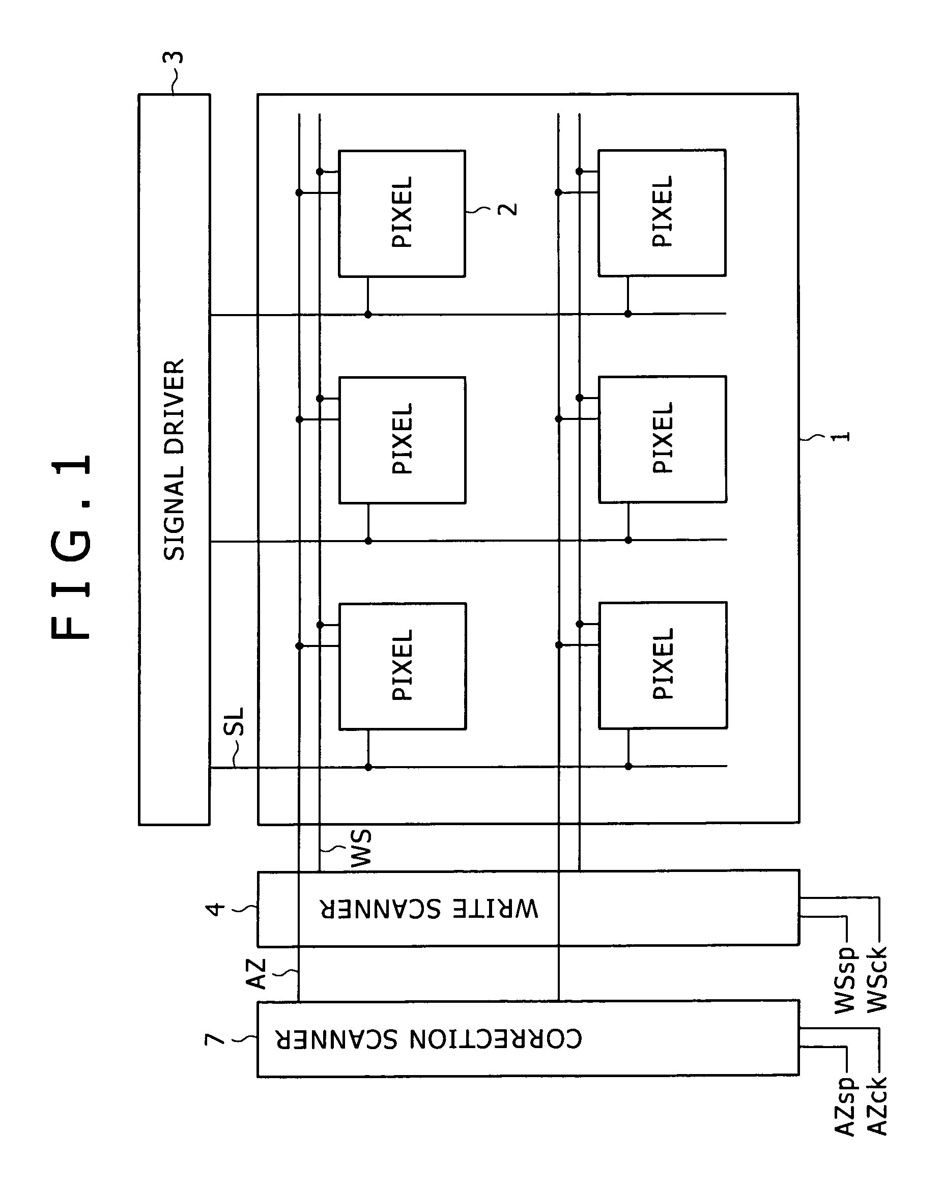
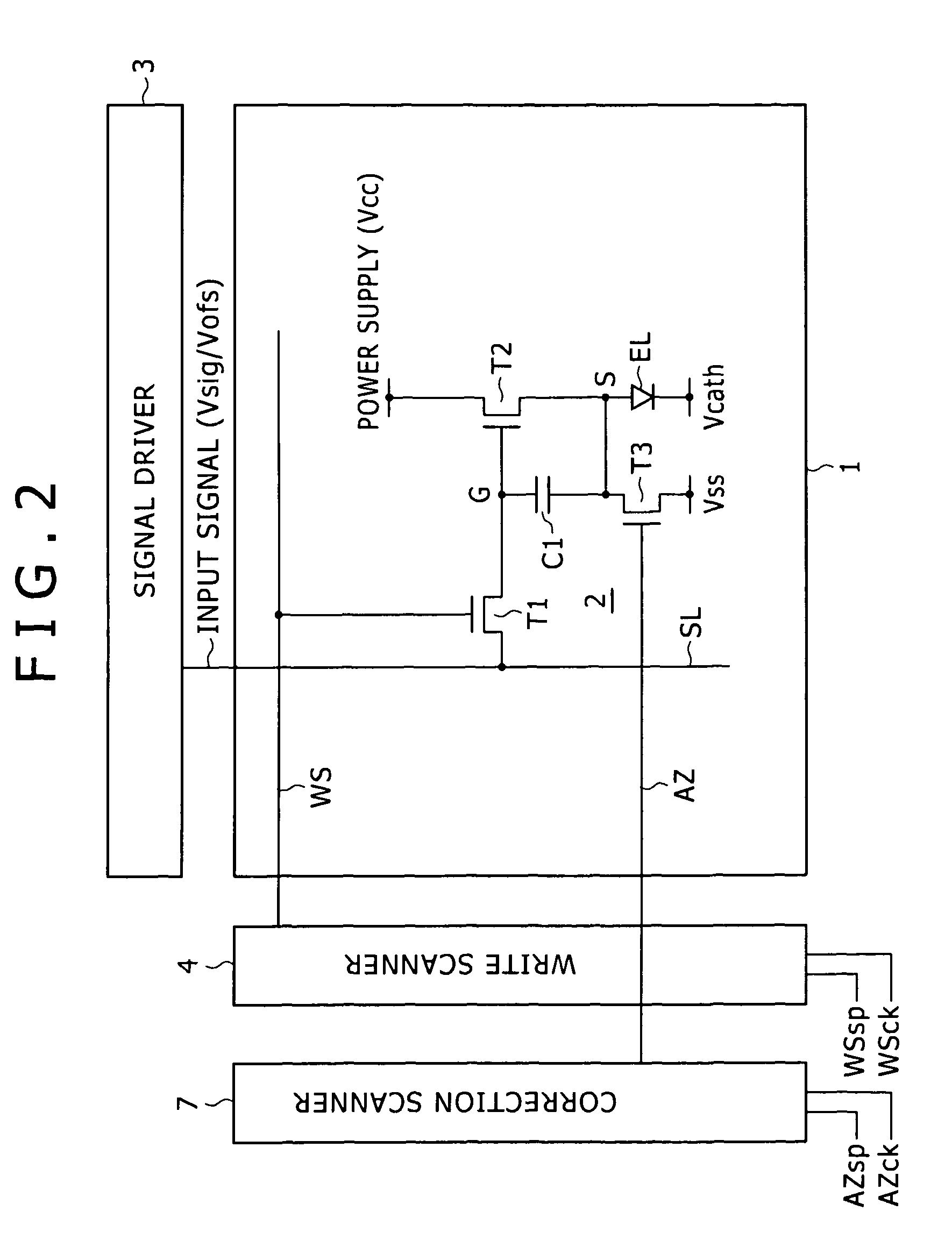
[0050]An embodiment of the present invention will be described in detail below with reference to the drawings. FIG. 1 is a block diagram showing the entire configuration of a display device. This display device is a reference example according to a previously-developed technique as the basis of the embodiment of the present invention. In order to clearly show the background of the present invention and facilitate understanding thereof, this previously-developed technique example will be described below as a part of the embodiment of the present invention. As shown in FIG. 1, this display device is basically composed of a pixel array part 1 and a drive part for driving the pixel array part 1. The pixel array part 1 includes scan lines WS disposed along the rows, scan lines AZ disposed along the rows, signal lines SL disposed along the columns, and pixels 2 that are disposed at the respective intersections of the scan lines WS and the signal lines SL so as to be arranged in a matrix. ...


PUM


Abstract

Disclosed herein is a display device including a pixel array part configured to include scan lines disposed along rows, signal lines disposed along columns, and pixels that are disposed at intersections of the scan lines and the signal lines and arranged in a matrix, each of the pixels having at least a sampling transistor, a drive transistor, a switching transistor, a hold capacitor, and a light-emitting element; and a drive part configured to include a scanner and a driver, the driver supplying a video signal to the signal lines along the columns.

Description

CROSS REFERENCES TO RELATED APPLICATIONS[0001]The present invention contains subject matter related to Japanese Patent Application JP 2007-333722 filed in the Japan Patent Office on Dec. 26, 2007, the entire contents of which being incorporated herein by reference.BACKGROUND OF THE INVENTION[0002]1. Field of the Invention[0003]The present invention relates to an active-matrix display device including light-emitting elements in its pixels. Furthermore, the present invention relates to electronic apparatus including such a display device.[0004]2. Description of the Related Art[0005]In recent years, development of flat self-luminous display devices employing organic EL devices as light-emitting elements is being actively promoted. The organic EL device is based on a phenomenon that an organic thin film emits light in response to application of an electric field thereto. The organic EL (Electro Luminescence) device can be driven by application voltage of 10 V or lower, and thus has low ...

Claims


Application Information

Patent Timeline
Patent Type & Authority Patents(United States)
IPC IPC(8): G09G3/30
CPCG09G3/3233G09G3/3266G09G3/3291G09G2300/0819G09G2300/0842G09G2310/0256G09G2320/043
Inventor YAMAMOTO, TETSUROUCHINO, KATSUHIDE
Owner JOLED INC
Why Eureka
Try Eureka