

Thin film transistor and method for fabricating the same
- Summary
- Abstract
- Description
- Claims
- Application Information
AI Technical Summary
Benefits of technology
Problems solved by technology
Method used
Image

Examples
Embodiment Construction
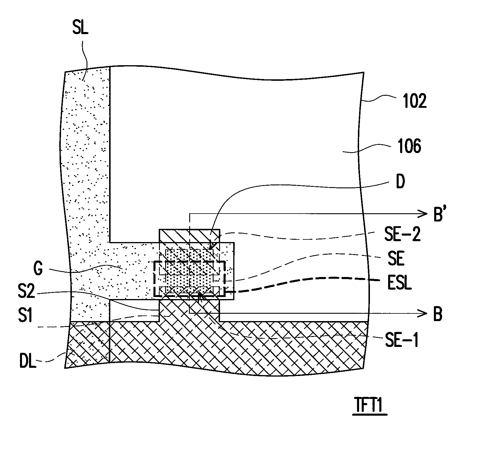
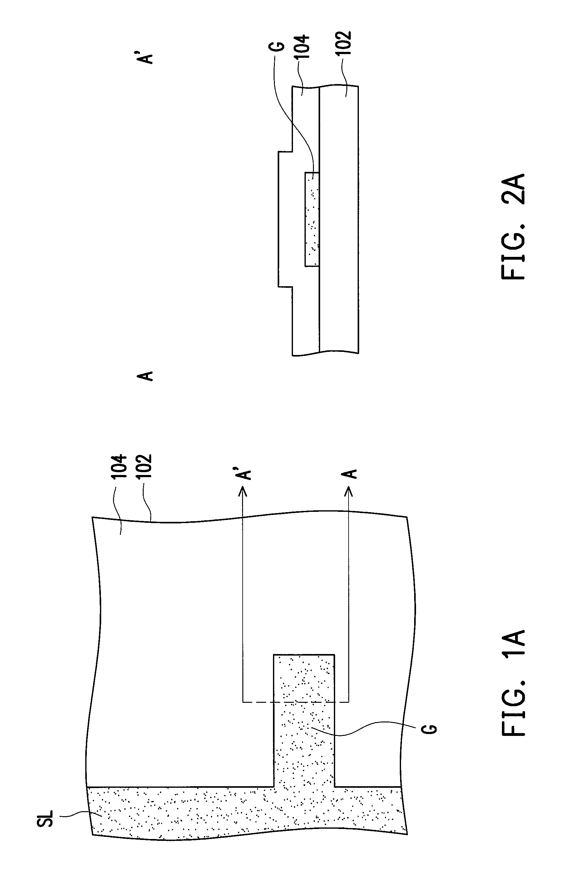
[0028]FIG. 1A through FIG. 1E are schematic top views illustrating a method for fabricating a thin film transistor according to an embodiment of the present invention. FIG. 2A through FIG. 2E are schematic cross-sectional views illustrating a method for fabricating a thin film transistor according to an embodiment of the present invention. Specially, FIG. 2A through FIG. 2E are schematic cross-sectional views respectively corresponding to FIG. 1A through FIG. 1E along a along a section line A-A′. Referring to FIG. 1A and FIG. 2A, a substrate 102 is first provided. The substrate 102 is used to carry elements, and a material of the substrate 102 may be glass, quartz, organic polymer or any other opaque / reflective material (e.g. wafers or ceramics) or any other suitable material.
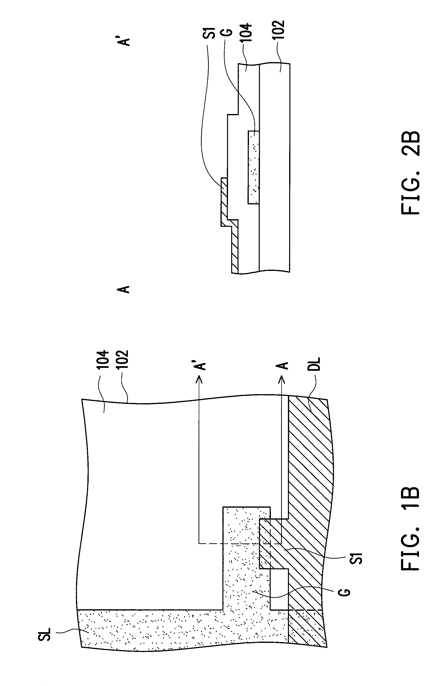
[0029]Then, a gate G is formed above the substrate 102. In the present embodiment, if the fabricated thin film transistor is applied to the display field, a scan line SL electrically connected with the gate G m...
PUM
 Abstract
Description
Claims
Application Information