

Esl TFT substrate structure and manufacturing method thereof
- Summary
- Abstract
- Description
- Claims
- Application Information
AI Technical Summary
Benefits of technology
Problems solved by technology
Method used
Image

Examples
Embodiment Construction
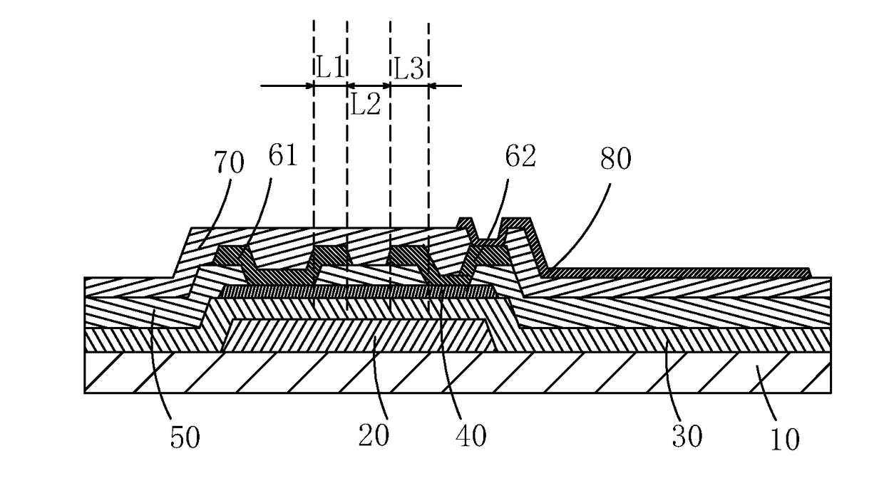
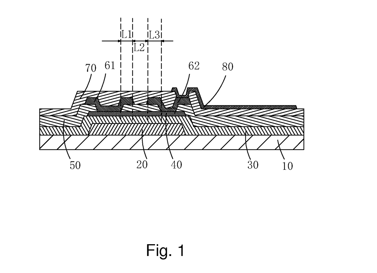
[0066]To further expound the technical solution adopted in the present invention and the advantages thereof, a detailed description is given to a preferred embodiment of the present invention and the attached drawings.
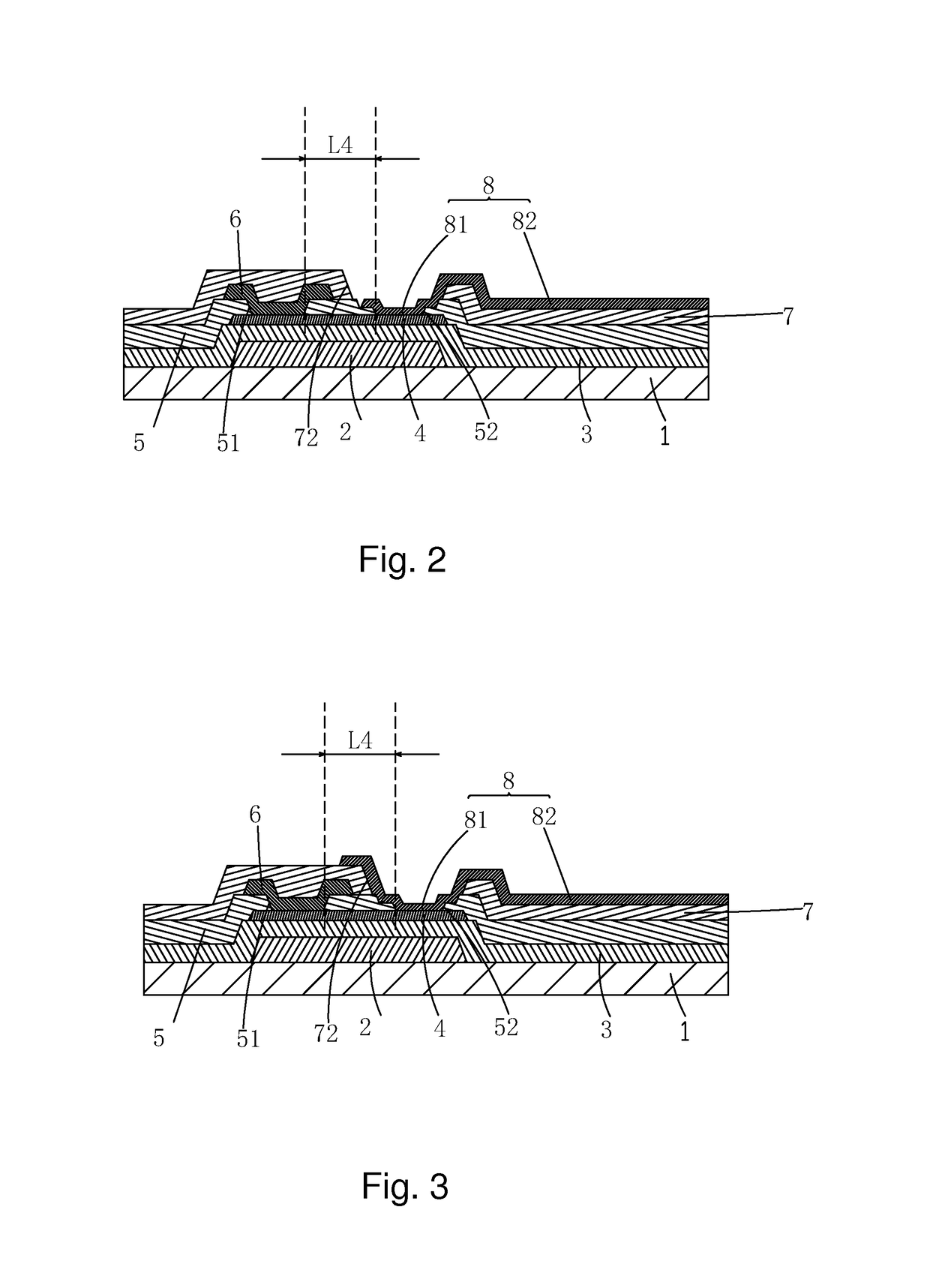
[0067]Firstly, the present invention provides an etch stop layer (ESL) thin-film transistor (TFT) substrate structure. FIG. 2 is a schematic view illustrating an ESL TFT substrate structure according to a first embodiment of the present invention. The ESL TFT substrate structure comprises:
[0068]a base plate 1;
[0069]a gate terminal 2 formed on the base plate 1;
[0070]a gate insulation layer 3 formed on the gate terminal 2 and the base plate 1;
[0071]an oxide semiconductor layer 4 located above the gate terminal 2 and formed on the gate insulation layer 2;
[0072]an etch stop layer 5 formed on the oxide semiconductor layer 4, wherein the etch stop layer 5 comprises a first via 51 and a second via 52 formed therein to respectively correspond to two side portions of the oxide ...
PUM
 Abstract
Description
Claims
Application Information