Field effect transistor

Active Publication Date: 2009-09-17
MITSUBISHI ELECTRIC CORP
View PDF16 Cites 29 Cited by
  • Summary
  • Abstract
  • Description
  • Claims
  • Application Information

AI Technical Summary

Benefits of technology

[0047]As described above, in accordance with the present invention, a field effect transistor exhibi

Problems solved by technology

In such HJFET 200, since the transistor has AlGaN/GaN hetero-junction therein, trade-off exists be

Method used


Image

  • Field effect transistor
  • Field effect transistor
  • Field effect transistor

Examples


first exemplary embodiment

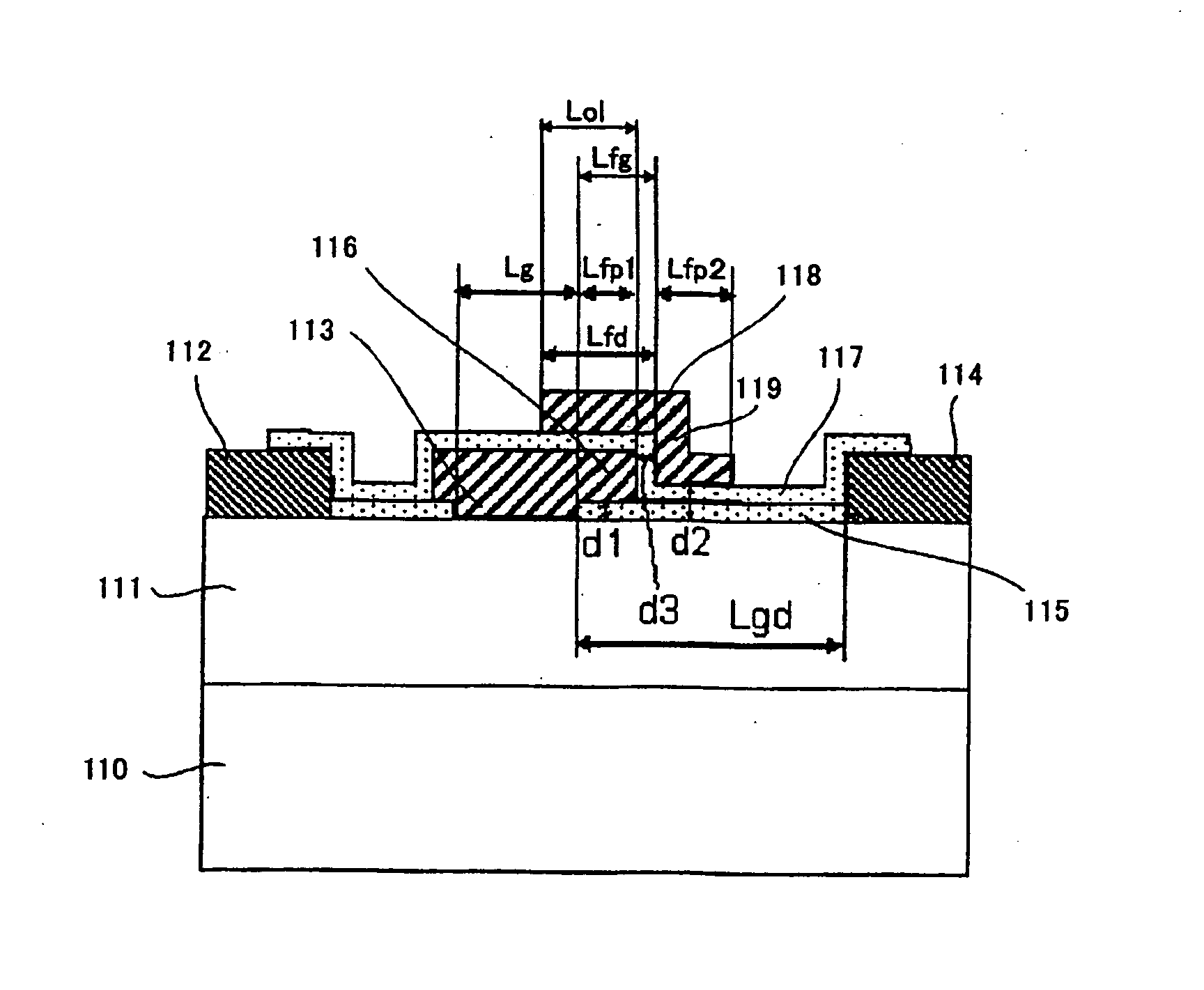
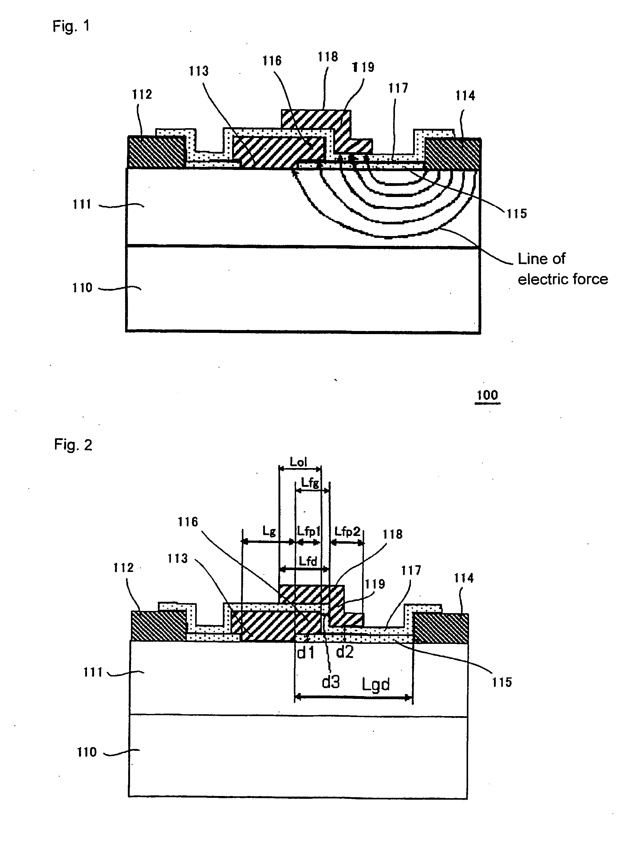
[0087]FIG. 1 is a cross sectional view showing the structure of a nitride semiconductor field effect transistor of the present exemplary embodiment. The field effect transistor 100 shown in FIG. 1 is a transistor which is of HJFET type using nitride semiconductor with a dual field plate structure.

[0088]This transistor comprises a layer structure made of Group III nitride semiconductor (nitride semiconductor 111) comprising hetero-junction, a source electrode 112 and a drain electrode 114 which are formed on a upper part of the nitride semiconductor 111 in a spaced manner, a gate electrode 113 placed between the source electrode 112 and the drain electrode 114, a first field plate (first field plate electrode 116) provided above the nitride semiconductor 111 in the region between the gate electrode 113 and the drain electrode 114 and isolated from the nitride semiconductor 111, and a second field plate (second field plate electrode 118) provided above the nitride semiconductor 111 an...

second exemplary embodiment

[0149]While explanation has been made in the first exemplary embodiment in connection with the case where there is employed the structure in which the lower surface (lower end) of the first field plate electrode 116 is located on the nitride semiconductor 111 side relative to the lower surface (lower end) of the shielding part 119. In the field effect transistors described in the first embodiment and exemplary embodiments succeeding thereto, there may be employed a structure in which the lower surface (lower end) of the shielding part 119 is located at the lower part relative to the lower surface (lower end) of the first field plate electrode 116, i.e., on the nitride semiconductor 111 side. In this exemplary embodiment, a transistor with such structure will be described.

[0150]FIG. 11 is a cross sectional view showing the structure of a field effect transistor of the present exemplary embodiment.

[0151]In the field effect transistor shown in FIG. 11, the lower end (lower surface) of ...

third exemplary embodiment

[0153]While explanation has been made in the aforementioned exemplary embodiments in connection with the integral type structure in which the gate electrode 113 and the first field plate electrode 116 are integrally continuously formed, there may be employed a structure in which the gate electrode 113 and the first field plate electrode 116 are structurally separated into different members, and are electrically connected in isolation region (not shown) of the device. The present exemplary embodiment relates to a field effect transistor of such a structure.

[0154]FIG. 13 is a cross sectional view showing the structure of the field effect transistor of the present exemplary embodiment. In the field effect transistor shown in FIG. 13, the first field plate electrode 116 serves as an electric field control electrode provided in a manner spaced from the gate electrode 113.

[0155]Also in the present exemplary embodiment, similar advantages as that in the first exemplary embodiment can be ob...


PUM


Abstract

A field effect transistor (100) exhibiting good performance at high voltage operation and high frequency includes a first field plate electrode (116) and a second field plate electrode (118). The second field plate electrode includes a shielding part (119) located in the region between the first field plate electrode and a drain electrode (114), and serves to shield the first field plate electrode from the drain electrode. When in the cross sectional view in the gate length direction, the length in the gate length direction of an overlap region where the second field plate electrode (118) overlap the upper part of a structure including the first field plate electrode and a gate electrode (113) is designated as Lol, and the gate length is Lg, the relation expressed as 0≦Lol/Lg≦1 holds.

Description

TECHNICAL FIELD[0001]The present invention relates to a field effect transistor using Group III nitride semiconductor. In particular, the present invention relates to a structure fit for attaining excellent high frequency characteristic and high voltage performance in a hetero-junction field effect transistor utilizing Group III nitride semiconductor.RELATED ART[0002]As a field effect transistor using Group III nitride semiconductor, there has been reported a field effect transistor as shown in FIG. 17 (Non-Patent Document 1:Y. Ando, et al., 2001 International Electron Devices Meeting Digest (IEDM 01) pp. 381-384). FIG. 17 is a cross sectional view showing the structure of a Hetero-Junction Field Effect Transistor (which will be simply referred to as HJFET hereinafter).[0003]In this HJFET 200, an AIN buffer layer 211 is formed on a sapphire substrate 209. A GaN channel layer 212 is formed on the AIN buffer layer 211, and an AlGaN electron supply layer 213 is formed thereon. A source...

Claims


Application Information

Patent Timeline
IPC IPC(8): H01L29/80
CPCH01L29/2003H01L29/402H01L29/812H01L29/7787H01L29/802H01L29/404
Inventor MIYAMOTO, HIRONOBUANDO, YUJIOKAMOTO, YASUHIRONAKAYAMA, TASUOINOUE, TAKASHIOTA, KAZUKIWAKEJIMA, AKIOKASAHARA, KENSUKEMURASE, YASUHIROMATSUNAGA, KOHJIYAMANOGUCHI, KATSUMISHIMAWAKI, HIDENORI
Owner MITSUBISHI ELECTRIC CORP
Why Eureka
Try Eureka