Two Transistor SONOS Flash Memory

Active Publication Date: 2016-10-06
NEO SEMICON
View PDF4 Cites 6 Cited by
  • Summary
  • Abstract
  • Description
  • Claims
  • Application Information

AI Technical Summary

Benefits of technology

This patent describes a new flash memory device that has two memory cells, each containing a control gate and a select gate transistor. The transistors have a channel region that is less than 90 nm in length. The method for programming the memory cells involves setting a bias level and a voltage to generate electron / hole pairs in a drain region of the control gate transistor, while the select gate transistor passes a voltage to the control gate transistor to allow a punch-through current to flow in the channel region. The method also includes setting a gate voltage to inject electrons into a charge-trapping layer of the control gate transistor using Punch-Through-Assisted-Hot-Electron (PAHE) injection. The technical effects of this patent are reduced punch-through voltage during programming, which allows for a more efficient programming process, and a significant reduction in channel length, which improves performance and reliability of the flash memory cells.

Problems solved by technology

However, during programming, the cell's channel has to sustain a 5V punch-through voltage and therefore the channel length of the conventional 2T SONOS cell cannot be scaled down below a set limit.
This increases the die size and cost and is particularly not suitable for lower density applications.
The high VDS requirement also significantly limits the scalability of the cell's channel length and therefore the overall array size.
Again, the high VDS requirement significantly limits the scalability of the cell's channel length.
As a result, the overall size cannot be reduced below that which is necessary to support the required channel length of the cells.

Method used


Image

  • Two Transistor SONOS Flash Memory
  • Two Transistor SONOS Flash Memory
  • Two Transistor SONOS Flash Memory

Examples


Embodiment Construction

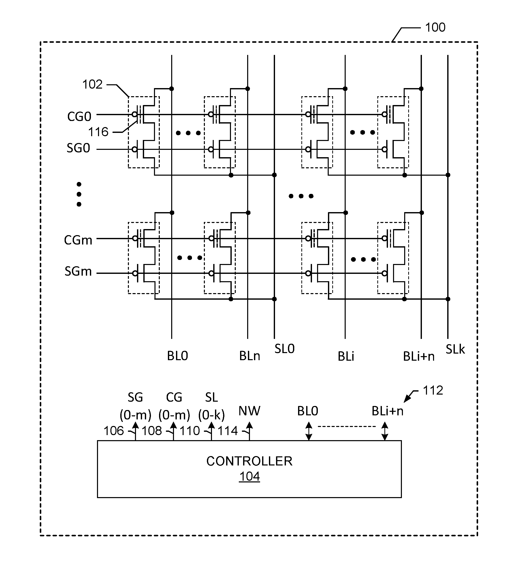
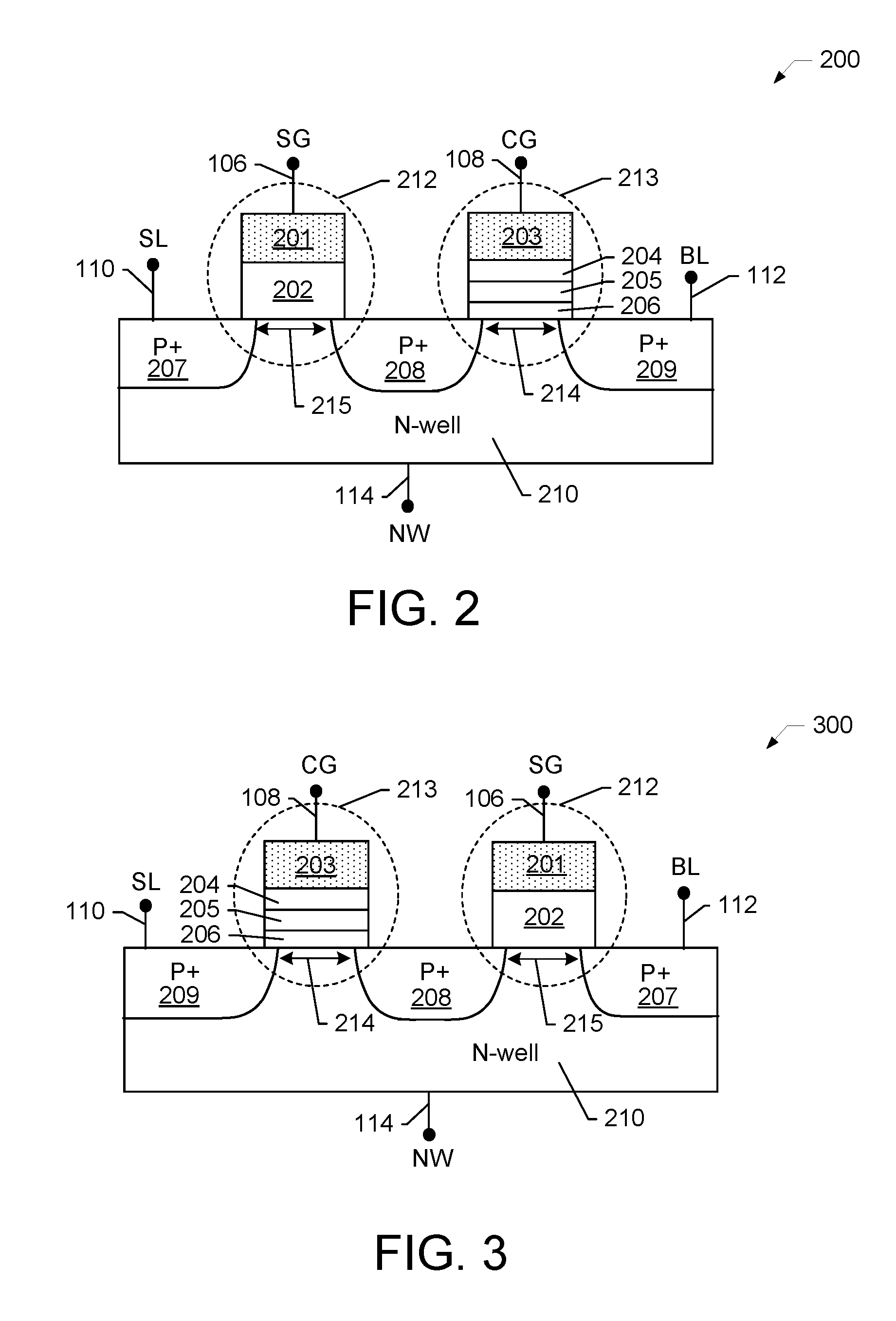
[0024]Exemplary embodiments of the present invention are described herein in the context of a process, device, method, and apparatus for providing a novel flash memory utilizing 2T memory cells, such as SONOS cells or floating gate cells.

[0025]Those of ordinary skilled in the art will realize that the following detailed description is illustrative only and is not intended to be in any way limiting. Other embodiments of the present invention will readily suggest themselves to such skilled persons having the benefit of this disclosure. Reference will now be made in detail to implementations of the exemplary embodiments of the present invention as illustrated in the accompanying drawings. The same reference indicators (or numbers) will be used throughout the drawings and the following detailed description to refer to the same or like parts.

[0026]It should be noted that the exemplary embodiments are not limited to SONOS cells only and can be applied with any other type of charge-trappin...


PUM


Abstract

A two transistor SONOS flash memory is disclosed. In one aspect, an apparatus, includes a control gate transistor having source and drain diffusions deposited in an N-well, a charge-trapping region formed on the N-well that overlaps the source and drain diffusions, and a control gate formed on the charge-trapping region. A channel region of the N-well between the source and drain diffusions is less than 90 nm in length. The apparatus also includes a select gate transistor having a select source diffusion deposited in the N-well. A drain side of the select gate transistor shares the source diffusion. A channel region of the N-well between the select source diffusion and the source diffusion also is less than 90 nm in length.

Description

PRIORITY[0001]This application claims the benefit of priority based upon U.S. Provisional Patent Application having Application No. 62 / 143,143, filed on Apr. 5, 2015, and entitled “2T SONOS Flash Memory,” which is hereby incorporated herein by reference in its entirety.FIELD OF THE INVENTION[0002]The exemplary embodiments of the present invention relate generally to the field of semiconductors and integrated circuits, and more specifically to memory and storage devices.BACKGROUND OF THE INVENTION[0003]A tradition flash memory may comprise silicon-oxide-nitride-oxide-silicon (SONOS) cells having a two-transistor (2T) structure that prevents over-erase and drain voltage disturb. However, during programming, the cell's channel has to sustain a 5V punch-through voltage and therefore the channel length of the conventional 2T SONOS cell cannot be scaled down below a set limit. For example, the 2T SONOS cell may be programmed using Channel-Hot-Hole-Induced-Hot-Electron (CHHIHE) injection. ...

Claims


Application Information

Patent Timeline
IPC IPC(8): G11C16/04G11C16/06H01L27/115
CPCG11C16/0433H01L27/11573G11C16/06G11C16/0466H01L27/11526G11C16/10H10B43/35
Inventor HSU, FU-CHANG
Owner NEO SEMICON
Why Eureka
Try Eureka