

Vertical npn device in bcd process and its manufacturing method
A vertical type and device technology, applied in semiconductor/solid-state device manufacturing, semiconductor devices, electrical components, etc., can solve problems affecting devices, narrowing the width of the base region 104, etc., and achieve the effect of reducing process costs
- Summary
- Abstract
- Description
- Claims
- Application Information
AI Technical Summary
Problems solved by technology
Method used
Image

Examples
Embodiment B
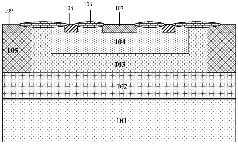
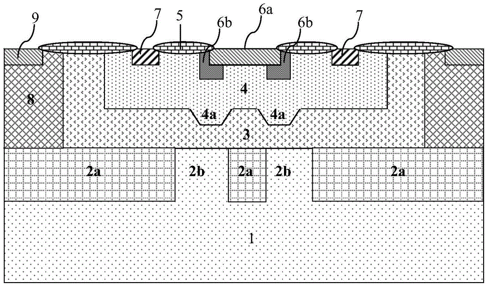
[0035] Such as figure 2 Shown is a schematic structural view of the vertical NPN device in the BCD process of the embodiment of the present invention; the vertical NPN device in the BCD process of the embodiment of the present invention includes:
[0036] The N-type buried layer is formed on the P-type silicon substrate 1, and the N-type buried layer is divided into a buried layer implanted region 2a and a buried layer non-implanted region 2b, and the doping concentration of the buried layer implanted region 2a is higher than that of the buried layer implanted region 2a The doping concentration of the buried layer non-implanted region 2b, the N-type impurity of the buried layer implanted region 2a is formed by N-type ion implantation, the N-type impurity of the buried layer non-implanted region 2b is formed by the buried layer implanted region 2a N-type impurities are formed by lateral diffusion.
[0037] An N-type epitaxial layer 3 is formed on the surface of the N-type bur...
PUM
 Abstract
Description
Claims
Application Information