Check patentability & draft patents in minutes with Patsnap Eureka AI!

Semiconductor integrated circuit

a technology of integrated circuits and semiconductors, applied in semiconductor devices, semiconductor/solid-state device testing/measurement, semiconductor/solid-state device details, etc., can solve the problem of difficult to provide a signal cell in the same column of the first row, and achieve the effect of reducing the increase in voltage drop

Active Publication Date: 2017-06-13
SONY CORP
View PDF2 Cites 0 Cited by
  • Summary
  • Abstract
  • Description
  • Claims
  • Application Information

AI Technical Summary

Benefits of technology

[0016]According to the present technology, a good effect that an increase in voltage drop can be reduced in a semiconductor integrated circuit can be exhibited.

Problems solved by technology

This is because if a power cell is provided in a second row, which is farther from the outer perimeter of the semiconductor chip, it is difficult to provide a signal cell in the same column of the first row due to mounting by wire bonding.

Method used


Image

  • Semiconductor integrated circuit
  • Semiconductor integrated circuit
  • Semiconductor integrated circuit

Examples


first embodiment (

[0027]1. First embodiment (an example in which a portion of a power supply ring and a portion of a ground ring are caused to protrude)

[0028]2. Second embodiment (an example in which power cells having different potentials are arranged adjacent to each other, and a portion of a power supply ring and a portion of a ground ring are caused to protrude)

third embodiment (

[0029]3. Third embodiment (an example in which a test pad is separated from an I / O cell, and a portion of a power supply ring and a portion of a ground ring are caused to protrude)

first embodiment

[0030]

[0031][Example Configuration of Semiconductor Integrated Circuit]

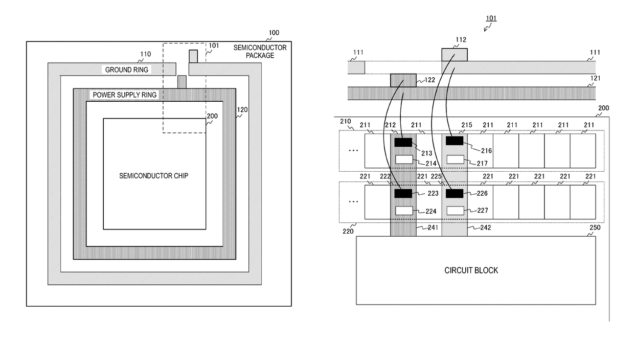
[0032]FIG. 1 is an example top view of a semiconductor integrated circuit in a first embodiment. The semiconductor integrated circuit includes a semiconductor package 100 and a semiconductor chip 200.

[0033]The semiconductor package 100 is a part that protects the semiconductor chip 200, and also distributes signals and power to the semiconductor chip 200. The semiconductor package 100 includes a ground ring 110 and a power supply ring 120.

[0034]The power supply ring 120 is an interconnect formed in a predetermined shape for supplying a power supply potential to the semiconductor chip 200, on a substrate of the semiconductor package 100 on which the semiconductor chip 200 is provided. For example, the power supply ring 120 is formed in the shape of a ring that surrounds the semiconductor chip 200 on the substrate of the semiconductor package 100.

[0035]The ground ring 110 is an interconnect formed in a predetermine...


PUM


Abstract

Provided is a semiconductor integrated circuit including: a plurality of first input / output cells arranged on a semiconductor integrated circuit substrate; a plurality of second input / output cells arranged on the semiconductor integrated circuit substrate along the plurality of first input / output cells; and a potential supply portion formed on a semiconductor package substrate, a portion of the potential supply portion protruding in a surface of the semiconductor package substrate, and configured to supply a predetermined potential to a target cell which is one of the plurality of first input / output cells and a cell neighboring the target cell among the plurality of second input / output cells through a region including the protruding portion.

Description

TECHNICAL FIELD[0001]The present technology relates to semiconductor integrated circuits. More particularly, the present technology relates to a semiconductor integrated circuit having an input / output cell which receives and outputs a signal and power supply.BACKGROUND ART[0002]There has in recent years been a demand for smaller and lighter electronic devices. Attempts have been made to increase the integration of a semiconductor integrated circuit included in an electronic device in order to, for example, reduce the size of the electronic device. A higher integration of a semiconductor integrated circuit is accompanied by an increase in the number of signals or power input to and output from the semiconductor integrated circuit. Therefore, a semiconductor package is used to efficiently distribute these signals or power.[0003]A semiconductor chip is provided on the substrate of a semiconductor package, and a power supply ring, ground ring, lead frame, and the like are provided aroun...

Claims


Application Information

Patent Timeline
Patent Type & Authority Patents(United States)
IPC IPC(8): H01L21/66H01L27/118H01L23/00H01L23/498
CPCH01L27/11898H01L22/32H01L23/49838H01L24/06H01L2224/05553H01L2224/06163H01L2224/48091H01L2224/49113H01L2224/49171H01L2924/00014H01L23/50
Inventor DANARDONO, DWI ANTONOSATO, MASAHIRO
Owner SONY CORP
Features
  • R&D
  • Intellectual Property
  • Life Sciences
  • Materials
  • Tech Scout
  • Unparalleled Data Quality
  • Higher Quality Content
  • 60% Fewer Hallucinations
Learn More