Array substrate, display panel and liquid crystal display device

a liquid crystal display and array substrate technology, applied in non-linear optics, instruments, optics, etc., can solve the problems of tremendously lowering the quality of array substrate and display panel, difficult to change the thickness of storage capacitor cst and the area of pixel electrodes, etc., to achieve the effect of increasing the aperture ratio of the display, ensuring the operation reliability, and reducing the thickness of the storage capacitor cs

Active Publication Date: 2018-05-22
WUHAN CHINA STAR OPTOELECTRONICS TECH CO LTD
View PDF12 Cites 0 Cited by
  • Summary
  • Abstract
  • Description
  • Claims
  • Application Information

AI Technical Summary

Benefits of technology

[0021]The array substrate further comprises an ohm contact layer, and the ohm contact layer is located between the first portion and the drain region, and is employed to reduce a contact resistance between the first portion and the drain region.
[0029]In the array substrate of the present invention, because the pixel electrode is electrically connected to the first portion of the active layer through the drain region, the first storage capacitor Cst1 and the second storage capacitor Cst2 are coupled in parallel to form a total storage Cst of the array substrate, and Cst=Cst1+Cst2, and thus to increase the total storage capacitor Cst of the array substrate, so as to avoid the issues of the cross talk and the Image Sticking due to the over small total storage capacitor Cst for promoting the quality of the array substrate.
[0031]Moreover, the first common electrode is electrically connected to the second common electrode and the pixel electrode is electrically connected to the first portion of the active layer, the first storage capacitor Cst1 and the second storage capacitor Cst2 are equipotential, and meanwhile, the charge and discharge operation of the second storage capacitor Cst2 is controllable, and thus, the charge and discharge operation of the first storage capacitor Cst1 is similarly controllable. Thus, under the premise that the array substrate increase the total storage capacitor Cst in the present invention, the charge and discharge operation of the first storage capacitor Cst1 added in the array substrate is controllable and stable. Moreover, the components of the first storage capacitor Cst1 and the second storage capacitor Cst2 are individually and independently located, which is also beneficial to make the first storage capacitor Cst1 and the second storage capacitor Cst2 more stable and more reliable in the operation.
[0032]In the display panel and the liquid crystal display device of this embodiment, because the array substrate is utilized, the total storage capacitor Cst of the array substrate can be increased under circumstance that the aperture ratio of the display is not reduced, so as the display panel can avoid the issues of the cross talk and the Image Sticking due to the over small total storage capacitor Cst to promote the quality of the display panel.

Problems solved by technology

In the condition of prior art, for satisfying the requirement of optical quality and the transmission rate, it is difficult to make change to the thickness of the storage capacitor Cst and the area of the pixel electrode.
The electrical quantity of each storage capacitor cannot maintain the normal working voltage of the pixel, and results in the issues of the cross talk and the Image Sticking, which tremendously lower the qualities of the array substrate and the display panel.

Method used


Image

  • Array substrate, display panel and liquid crystal display device
  • Array substrate, display panel and liquid crystal display device
  • Array substrate, display panel and liquid crystal display device

Examples


Embodiment Construction

[0038]Embodiments of the present invention are described in detail with the technical matters, structural features, achieved objects, and effects with reference to the accompanying drawings as follows. It is clear that the described embodiments are part of embodiments of the present invention, but not all embodiments. Based on the embodiments of the present invention, all other embodiments to those of ordinary skill in the premise of no creative efforts obtained, should be considered within the scope of protection of the present invention.

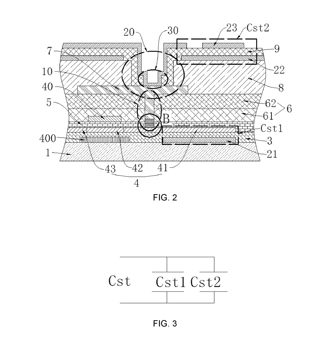
[0039]Please refer from FIG. 1 to FIG. 3. The embodiment of the present invention provides an array substrate, comprising:

[0040]a substrate 1;

[0041]forming a first common electrode 21 on the substrate 1;

[0042]a buffer layer 3 covering the first common electrode 21;

[0043]an active layer 4 formed on a surface of the buffer layer 3 away from the first common electrode 21, and the active layer 3 comprises a first portion 41 oppositely located to the fi...


PUM

PropertyMeasurementUnit
contact resistanceaaaaaaaaaa
concentrationaaaaaaaaaa
transparent conductiveaaaaaaaaaa

Abstract

The present invention discloses an array substrate, comprising a first storage capacitor and a second storage capacitor, and the first storage capacitor and the second storage capacitor are coupled in parallel to form a total storage capacitor of the array substrate to increase the total storage capacitor of the array substrate, so as to avoid the issues of the cross talk and the image residue due to the over small total storage capacitor for promoting the quality of the array substrate. The present invention further discloses a display panel utilizing the array substrate and a liquid crystal display panel utilizing the array substrate.

Description

CROSS REFERENCE[0001]This application claims the priority of Chinese Patent Application No. 201610098282.2, entitled “Array substrate, display panel and liquid crystal display device”, filed on Feb. 23, 2016, the disclosure of which is incorporated herein by reference in its entirety.FIELD OF THE INVENTION[0002]The present invention relates to a display technology field, and more particularly to an array substrate, a display panel and a liquid crystal display device.BACKGROUND OF THE INVENTION[0003]With the constant development of the TFT (Thin Film Transistor) liquid crystal display technology, the TFT display device based on LTPS (Low Temperature Poly-silicon) skill possessing properties of low power consumption, high resolution, fast response speed and high aperture ratio has already become the mainstream, and widely applied in kinds of electronic apparatuses, like being applied in the digital electronic apparatuses, such as liquid crystal television, smart phone, tablet and digi...

Claims


Application Information

Patent Timeline
Patent Type & Authority Patents(United States)
IPC IPC(8): G02F1/1362G02F1/1368G02F1/1343
CPCG02F1/136213G02F1/1368G02F1/136209G02F1/136227G02F1/136286G02F2202/104G02F1/134363G02F2001/13685G02F2201/121G02F2201/123G02F2201/40G02F1/13685G02F1/134372
Inventor LIU, YUANFU
Owner WUHAN CHINA STAR OPTOELECTRONICS TECH CO LTD
Why Eureka
Try Eureka