
Method for growing high-antistatic LED (light-emitting diode) by adopting metal organic compound vapor phase epitaxy technology
An organic compound, light-emitting diode technology, applied in chemical instruments and methods, crystal growth, single crystal growth, etc., can solve the problems of limited effect, high additional cost, complicated process flow, etc., to increase the built-in capacitance and improve the expansion effect. , the effect of increasing the hole concentration
Patent Information
- Authority / Receiving Office
- CN · China
- Current Assignee / Owner
- Publication Date
- 2012-01-25
- Estimated Expiration
- Not applicable · inactive patent
Smart Images
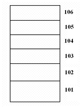
Figure 1 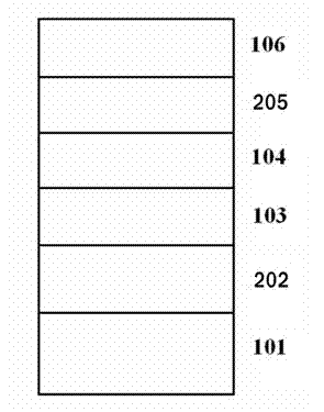
Figure 2 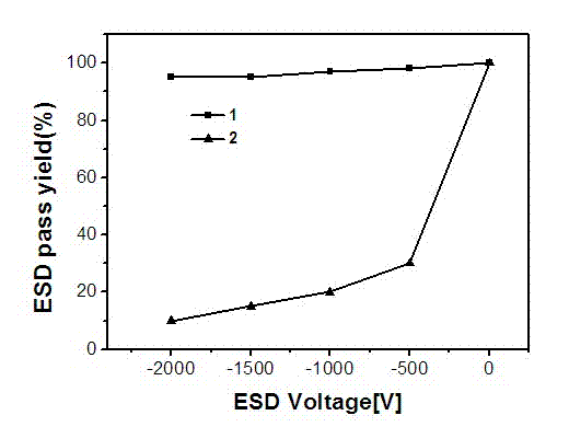
Figure 3
Abstract
Description
technical field
[0001] The invention relates to a method for manufacturing a light-emitting diode, in particular to a method for growing a light-emitting diode of a gallium nitride (GaN)-based III-V nitride semiconductor material with high antistatic ability by using metal organic compound vapor phase epitaxy (MOCVD) technology , Belonging to the field of semiconductor optoelectronic technology. Background technique
[0002] Gallium nitride (GaN)-based semiconductor materials are the third-generation semiconductor materials after silicon and gallium arsenide, and have developed rapidly in recent years. Group III nitrides, including GaN, InN, AlN, and ternary and quaternary alloys are direct bandgap wide bandgap semiconductor materials. The bandgap width of group III nitride materials at room temperature is continuously adjustable from 0.75eV of indium nitride (InN) to 3.4eV of gallium nitride (GaN) to 6.2eV of aluminum nitride (AlN), covering from infrared to ultraviolet I...
Examples
Embodiment 1
[0039] Aixtron, close-coupled vertical reaction chamber MOCVD growth system, was used. Trimethylgallium (TMGa), trimethylindium (TMIn), trimethylaluminum (TMAl) were used as group III sources during the growth process, and ammonia (NH 3 ) as the V group source, silane (SiH4) as the n-type doping source, and dimagnesium (Cp2Mg) as the p-type doping source, first heat the sapphire AlO3 substrate 101 to 1100 in the MOCVD reaction chamber , at H 2 5 minutes, then lower the temperature to 530~550 On Al2O3 substrates, high chamber pressure, hydrogen (H 2 ) atmosphere, the GaN buffer layer after three-dimensional growth of 20-30 nm, at 1000-1500 grow a 4 μm thick n-GaN layer 102 under nitrogen (N 2 ) atmosphere, at 750~850 grown 15 nm thick with an electron concentration of 10 19 cm -3 n-In 0.1 Ga 0.9 N (15nm) insertion layer 103, followed by growth of 10 cycles of In 0.18 Ga 0.82 N (2.5nm) / GaN (15nm) multiple quantum well active region 104'. on the active area, under...
Embodiment 2
[0041] Aixtron, close-coupled vertical reaction chamber MOCVD growth system was used. Trimethylgallium (TMGa), trimethylindium (TMIn), trimethylaluminum (TMAl) were used as group III sources during the growth process, and ammonia (NH 3 ) as the V group source, silane (SiH4) as the n-type doping source, and dimagnesium (Cp2Mg) as the p-type doping source, first heat the sapphire AlO3 substrate 101 to 1100 in the MOCVD reaction chamber , at H 2 5 minutes, then lower the temperature to 530~550 On Al2O3 substrates, high chamber pressure, hydrogen (H 2 ) atmosphere, the GaN buffer layer after three-dimensional growth of 20-30 nm, at 1000-1500 grow a 4 μm thick n-GaN layer 102 under nitrogen (N 2 ) atmosphere, at 750~850 Under multi-cycle growth, the electron concentration is 10 19 cm -3 n-In 0.1 Ga 0.9 N (2.5nm) / GaN (5nm) superlattice insertion layer 203, the number of periods of the superlattice is 10, and then grows 10 periods of In 0.18 Ga 0.82 N (2.5nm) / GaN (15nm...