
Discrete double rectangular gate-controlled source-drain resistive switching transistor of double conductivity type and manufacturing method thereof
A conductivity type, rectangular gate technology, applied in semiconductor/solid-state device manufacturing, transistors, semiconductor devices, etc.
Patent Information
- Authority / Receiving Office
- CN · China
- Patent Type
- Patents(China)
- Current Assignee / Owner
- Publication Date
- 2019-11-22
Smart Images
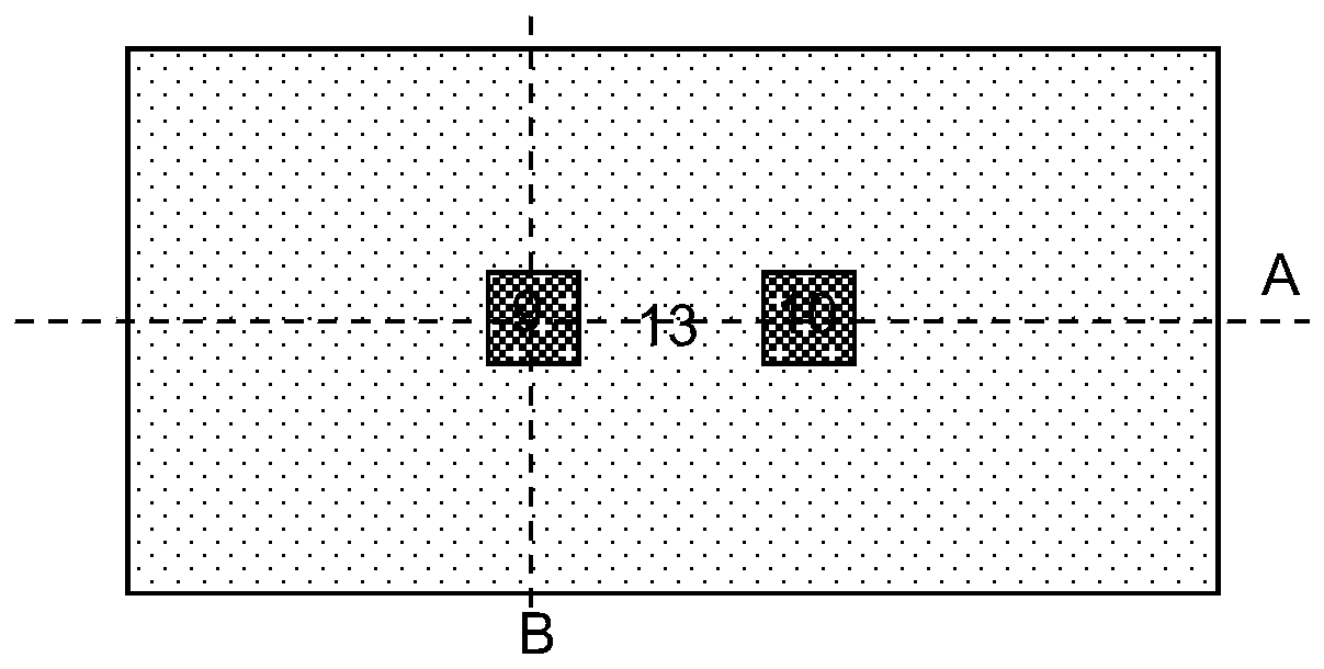
Figure 1 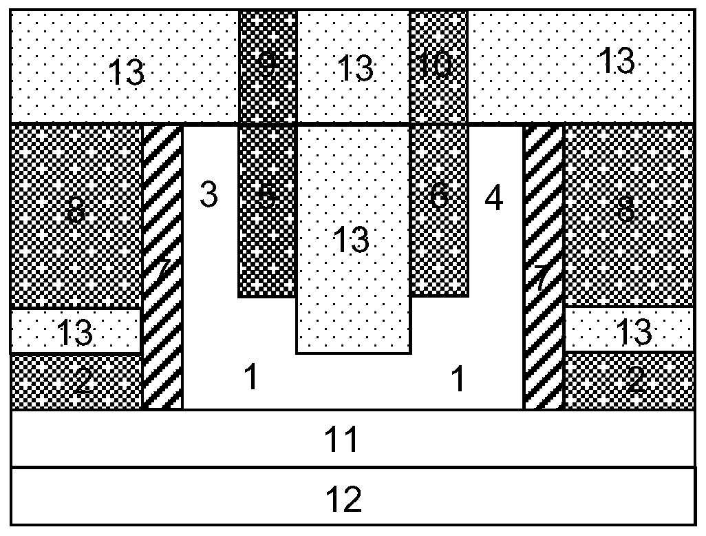
Figure 2 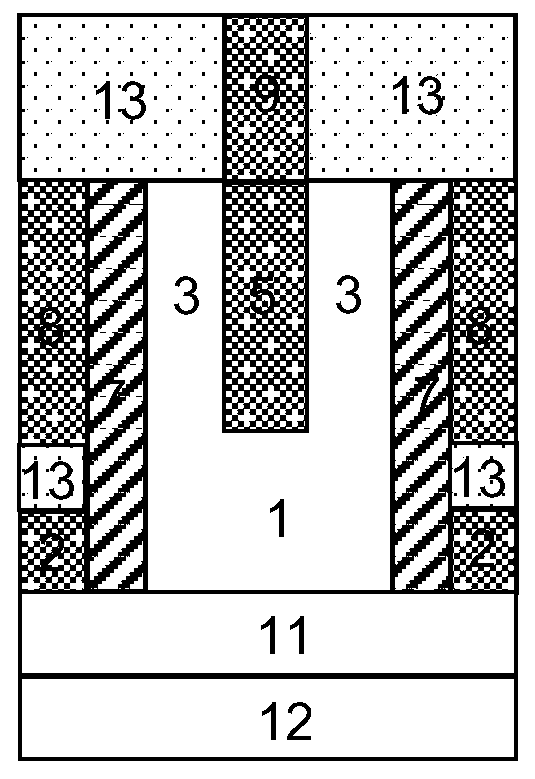
Figure 3
Abstract
Description
technical field
[0001] The invention relates to the field of ultra-large-scale integrated circuit manufacturing, in particular to a dual-conduction type discrete double rectangular gate-controlled source-drain resistive transistor with low leakage current suitable for low-power integrated circuit manufacturing and a manufacturing method thereof. Background technique
[0002] When ordinary tunneling field effect transistors are used as switching devices, the tunneling mechanism of carriers is used, which can make the subthreshold swing of ordinary tunneling field effect transistors better than the 60mV / dec limit of MOSFETs type devices. However, tunneling field effect transistors based on silicon-based materials have limited tunneling probability due to the limited band gap. Compared with MOSFETs, it is difficult to generate a conduction current of the same order. More seriously, the source and drain electrodes Doping with impurities of different conductivity types, the asymm...
Examples
Embodiment Construction
[0070] Below in conjunction with accompanying drawing, the present invention will be further described:
[0071] Such as figure 1 , figure 2 with image 3 As shown, a dual-conductivity type discrete double rectangular gate-controlled source-drain resistance switching transistor includes a silicon substrate 12 of an SOI wafer, and the silicon substrate 12 of the SOI wafer is a substrate insulating layer 11 of the SOI wafer. Above the substrate insulating layer 11 of the wafer is a part of the single crystal silicon film 1, the rectangular conductivity type selection gate 2 and the insulating dielectric barrier layer 13; wherein, the single crystal silicon film 1 has an impurity concentration lower than 10 16 cm -3The monocrystalline silicon semiconductor material has a U-shaped groove structure; the outer sides of the vertical parts on the left and right sides of the U-shaped groove structure formed by the single-crystal silicon film 1 are gate electrode insulating layers 7...