
Transmissive or reflective liquid crystal display and process for its manufacture
Patent Information
- Authority / Receiving Office
- US · United States
- Current Assignee / Owner
- Publication Date
- 2005-05-12
- Estimated Expiration
- Not applicable · inactive patent
Smart Images
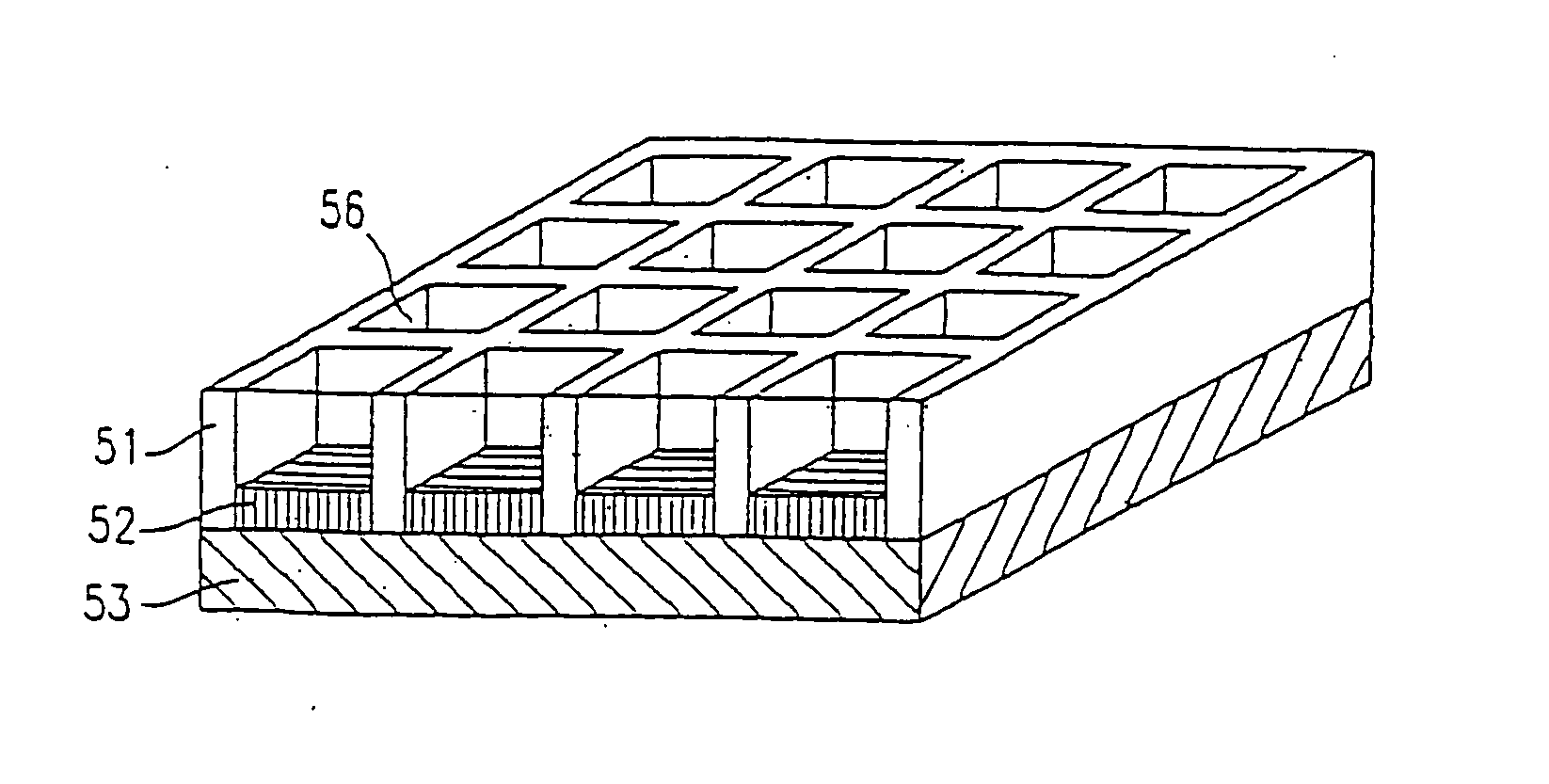
Figure 1 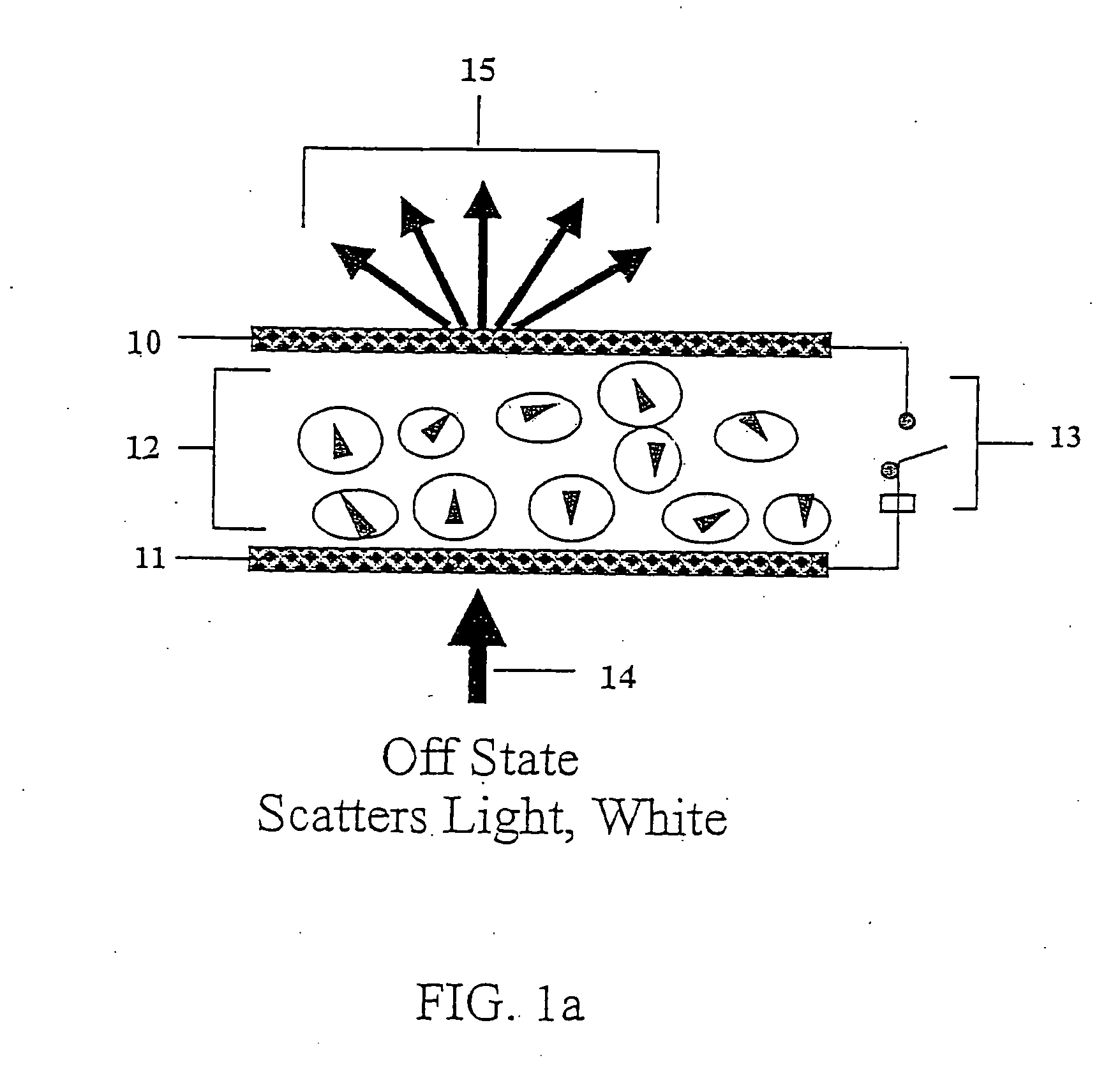
Figure 2 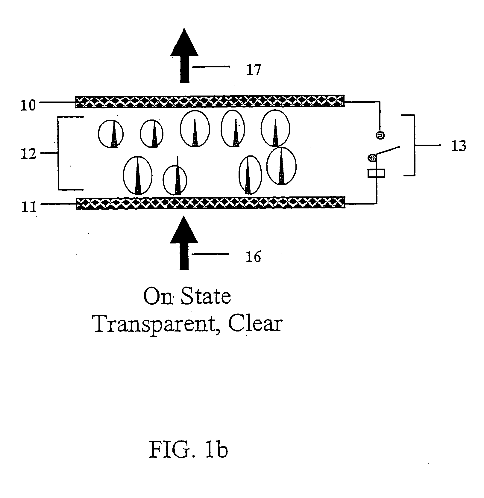
Figure 3
Abstract
Description
[0001] This application is a continuation-in-part of U.S. application Ser. No. 10 / 794,318, filed Mar. 5, 2004, which is a continuation-in-part of U.S. application Ser. No. 09 / 759,212, filed Jan. 11, 2001, both of which are incorporated herein by reference in their entirety.FIELD OF THE INVENTION
[0002] This invention relates to liquid crystal displays comprising cells of well-defined shape, size and aspect ratio, which are filled with liquid crystals, preferably with a guest dye, and novel processes for their manufacture. BACKGROUND OF THE INVENTION
[0003] A polymer dispersed liquid crystal (PDLC) display usually comprises two transparent plates with electrodes placed opposing each other, separated by using spacers. A thin film of PDLC is enclosed between the two plates. The PDLC film may be up to 200 micron thick, but usually having a thickness of between 2 microns and 50 microns. The cell is hermetically sealed in order to eliminate oxygen and moisture, both of which may chemicall...
Examples
example 1
Preparation of Microcups by Microembossing
[0105] The composition shown in Table 1 was coated with a Myrad bar #6 coated onto a 2 mil PET film precoated with an ITO conductor layer from Sheldahl (Northfield, Minn.). A pre-patterned (4×4×4 microns) cobalt nickel male mold and a mold release Frekote 700-NC from Henkel were used for microembossing. The coating thickness was controlled to be about 5 microns. The coated film was then embossed by the stencil using a pressure roller at 90° C. The coating was then UV-cured for about 1 minute through the Mylar film using a Cure Zone exposure unit (ADAC Technologies) equipped with a metal fluoride lamp with an intensity of 80 mW / cm2 at 365 nm. The embossed film was then released from the mold to reveal well-defined (4×4×4 microns) microcups. The microembossing was carried out using the GBC Laminator at 90° C.
TABLE 1UV-curable Acrylate Formulation for MicrocupsNo.DescriptionIngredientSupplierParts1EpoxyEbecryl 600UCB Chemicals55acrylate2Poly...
example 2
Preparation of Microcups by Microembossing
[0106] The same as Example 1 except the formulation shown in Table 2 was coated and embossed with a male mold of 4×4×4 microns.
TABLE 2UV-curable Acrylate Formulation for MicrocupsNo.DescriptionIngredientSupplierParts1Epoxy acrylateEbecryl 600UCB Chemicals502Polyester acrylateEbecryl 830UCB Chemicals153Urethane acrylateEbecryl 6700UCB Chemicals104Silicon acrylateEbecryl 350UCB Chemicals55MonomerPolyAldrich5(ethylene glycol)methacrylate6MonomerSartomer SR238Sartomer57MonomerSartomer SR306Sartomer58MonomerSartomer SR351Sartomer59PhotoinitiatorIrgacure 907Ciba0.510SolventMEKAldrich300
example 3
Preparation of Microcups by Microembossing
[0107] The composition shown in Table 3 was laminated using a pressure roller between a 2 PET film precoated with an ITO conductor layer, and a pre-patterned (4×4×4 microns) cobalt nickel mold. The PET / ITO film was treated with a corona discharge (Electro-Technic Products, Model BD-10A, Chicago, Ill.) for 5 sec. The cobalt nickel mold was pretreated with a mold release Frekote 750-NC. The coating was then UV cured for 1 min through the PET / ITO film. The embossing film was then released from the mold to reveal well-defined (4×4×4 microns) microcups with a thickness of 5.5 microns as measured by a Mituyoto thickness gauge.
TABLE 3UV-curable Acrylate Formulation for MicrocupsNo.DescriptionIngredientSupplierParts1Epoxy acrylateEbecryl 600UCB Chemicals402Polyester acrylateEbecryl 830UCB Chemicals153Urethane acrylateEbecryl 6700UCB Chemicals104Silicon acrylateEbecryl 350UCB Chemicals55MonomerPolyAldrich15(ethylene glycol)methacrylate6MonomerSart...