
Receiver
Patent Information
- Authority / Receiving Office
- US · United States
- Current Assignee / Owner
- Publication Date
- 2007-04-12
- Estimated Expiration
- Not applicable · inactive patent
Smart Images
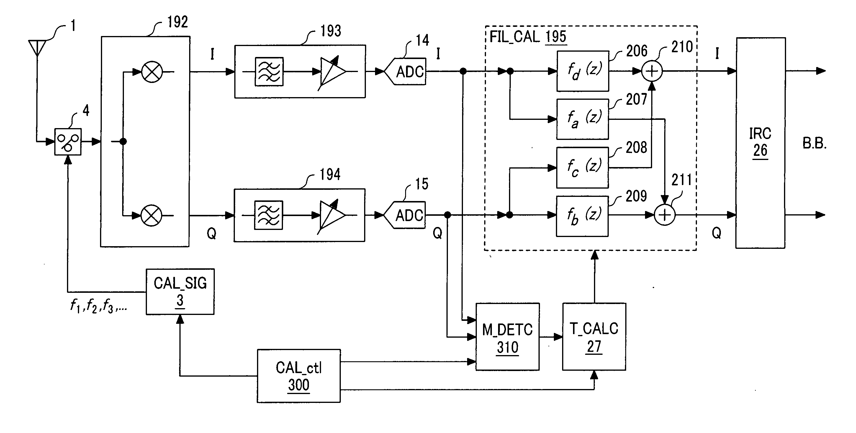
Figure 1 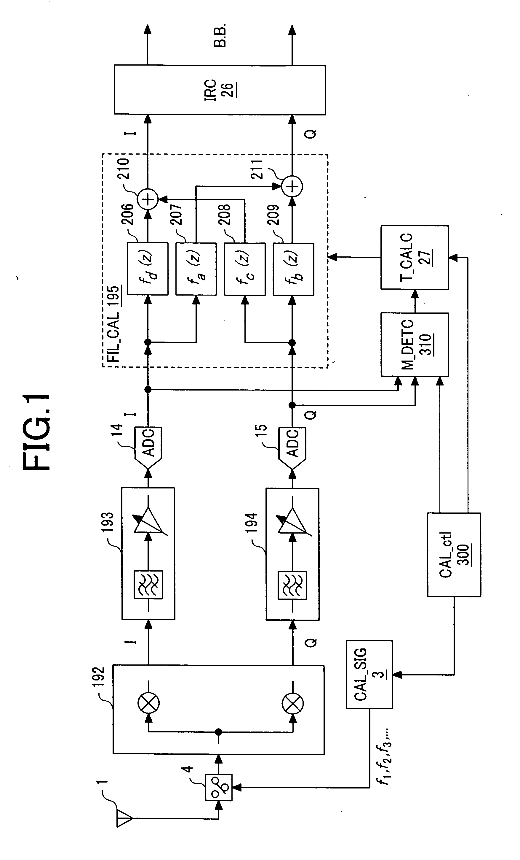
Figure 2 
Figure 3
Abstract
Description
CLAIM OF PRIORITY
[0001] The present application claims priority from Japanese application JP 2005-294444 filed on Oct. 7, 2005, the content of which is hereby incorporated by reference into this application. FIELD OF THE INVENTION
[0002] The present invention relates to a receiver and a mobile radio terminal used in a radio system, and particularly to a technology for calibrating, with a plurality of frequencies, amplitude mismatch and phase mismatch between an in-phase (I) component and a quadrature (Q) component in a quadrature demodulation signal. BACKGROUND OF THE INVENTION
[0003] In US Patent Application Publication of US 2005 / 0070236 A1, the technology is described for calibrating mismatch using a result on detecting phase and amplitude mismatch of a quadrature demodulation signal in order to realize high precision image rejection in a low IF receiver. Particularly, FIG. 6B of US 2005 / 0070236 A1 illustrates an example of an IQ mismatch correcting circuit. SUMMARY OF THE INVEN...
Examples
first embodiment
[0059] A first embodiment of the present invention will be explained with reference to FIG. 1 to FIG. 8.
[0060] First, FIG. 1 illustrates an example of structure of a receiver as the first embodiment of the present invention. A low IF receiver illustrated in FIG. 1 comprises an antenna 1, a calibration signal source 3, a switch 4, a quadrature mixer 192, an I component signal path 193, a Q component signal path 194, analog / digital converters (hereinafter referred to as “ADCs” (analog to digital converters)”14, 15, a filter mismatch calibrating circuit (FIL_CAL) 195, an image rejecting circuit (IRC) 26, a tap coefficient calculating circuit (T_CALC) 27, a calibration control circuit (CAL_ctl) 300, and a filter mismatch detecting circuit (M_DETC) 310.
[0061] This embodiment is characterized in comprising a filter mismatch calibrating unit including the calibration signal source 3, switch 4, tap coefficient calculating circuit (T_CALC) 27, filter mismatch calibrating circuit (FIL_CAL) ...
second embodiment
[0109] The second embodiment of the present invention will be described with reference to FIG. 9 to FIGS. 19A and 19B. This embodiment corresponds to a receiver employing the low IF system.
[0110] First, FIG. 9 illustrates a circuit structure of the low IF receiver as the second embodiment of the present invention. The low IF receiver illustrated in FIG. 9 comprises an antenna 1, an LNA 2, a calibration signal source 3, switches 4, 16 to 19, 22, 23, mixers 5, 6, an analog 90° phase shifter 7, an RF synthesizer 8, band-pass filters (BPFs) 9, 10, a control circuit 11, programmable gain amplifiers 12, 13, and analog / digital converters (ADCs) 14, 15. Moreover, the receiver also comprises a filter mismatch calibrating circuit (FIL_CAL) 20, a correction coefficient calculating circuit (C_CALC) 21, a memory (MEM) 24, an amplitude / phase mismatch calibrating circuit (GP_CAL) 25, an image rejecting circuit (IRC) 26, and a tap coefficient calculating circuit (T_CALC) 27.
[0111] This embodiment...
third embodiment
[0180]FIG. 20 shows an example of the other structure of the calibration signal source 3 as the third of the present invention. The calibration signal source 3 shown in the figure is constituted with inclusion of a crystal-controlled oscillator 118, a harmonics generating circuit 161, inverters 123, 124, differential amplifiers 125, 126 and switches 127, 128. The reference signal generated with the crystal-controlled oscillator 118 is inputted to the harmonics generating circuit 161. The harmonics generating circuit 161 of the third embodiment is formed of a PLL (Phase Locked Loop) and a fixed frequency divider with inclusion of a phase comparator (PD) 119, a low-pass filter (LPF) 120, a ring oscillator 121, a variable frequency divider (DIV) 122, and a frequency divider 162. The phase comparator (PD) 119, LPF 120, ring oscillator 121, and variable frequency divider (DIV) 122 form a PLL. In the phase comparator (PD) 119, the frequency of reference signal is compared with the frequen...