
Shielded bitline architecture for dynamic random access memory (DRAM) arrays
a dynamic random access memory and array technology, applied in the field of shielded bitline architecture for dram arrays, can solve the problems of increasing the required overall dram memory array area and concomitant increase in device cost, so as to reduce concomitant device cost, save power, and preserve the on-chip die area required
Patent Information
- Authority / Receiving Office
- US · United States
- Patent Type
- Applications(United States)
- Current Assignee / Owner
- Publication Date
- 2007-05-31
- Estimated Expiration
- Not applicable · inactive patent
Smart Images
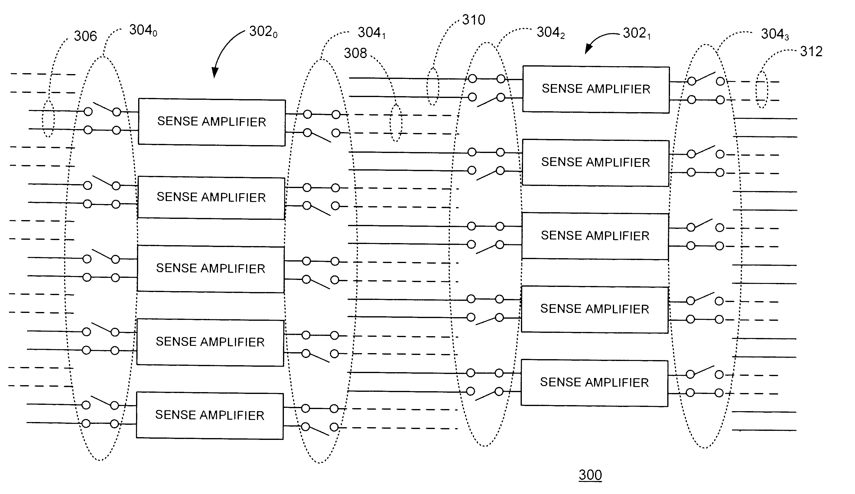
Figure 1 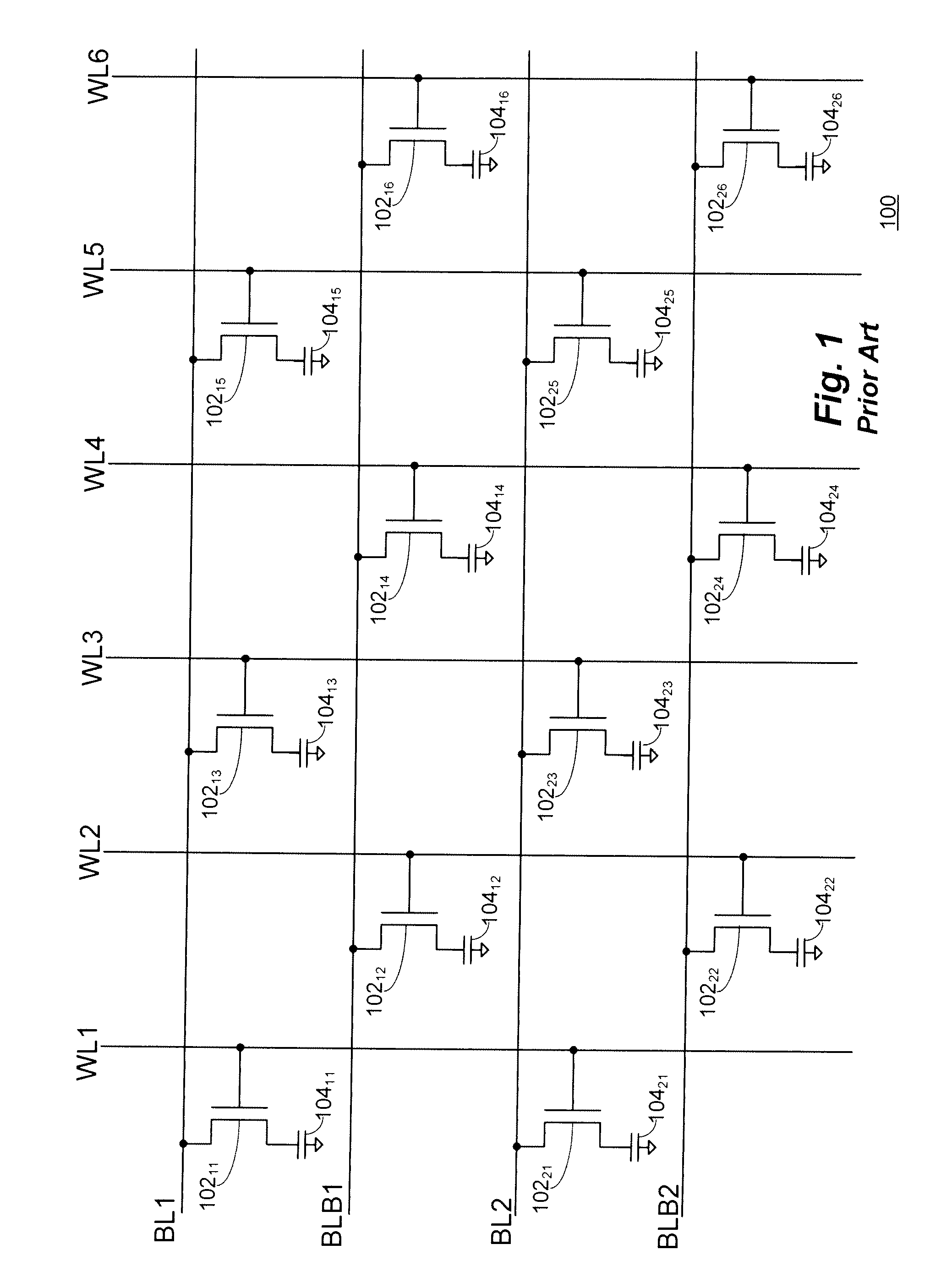
Figure 2 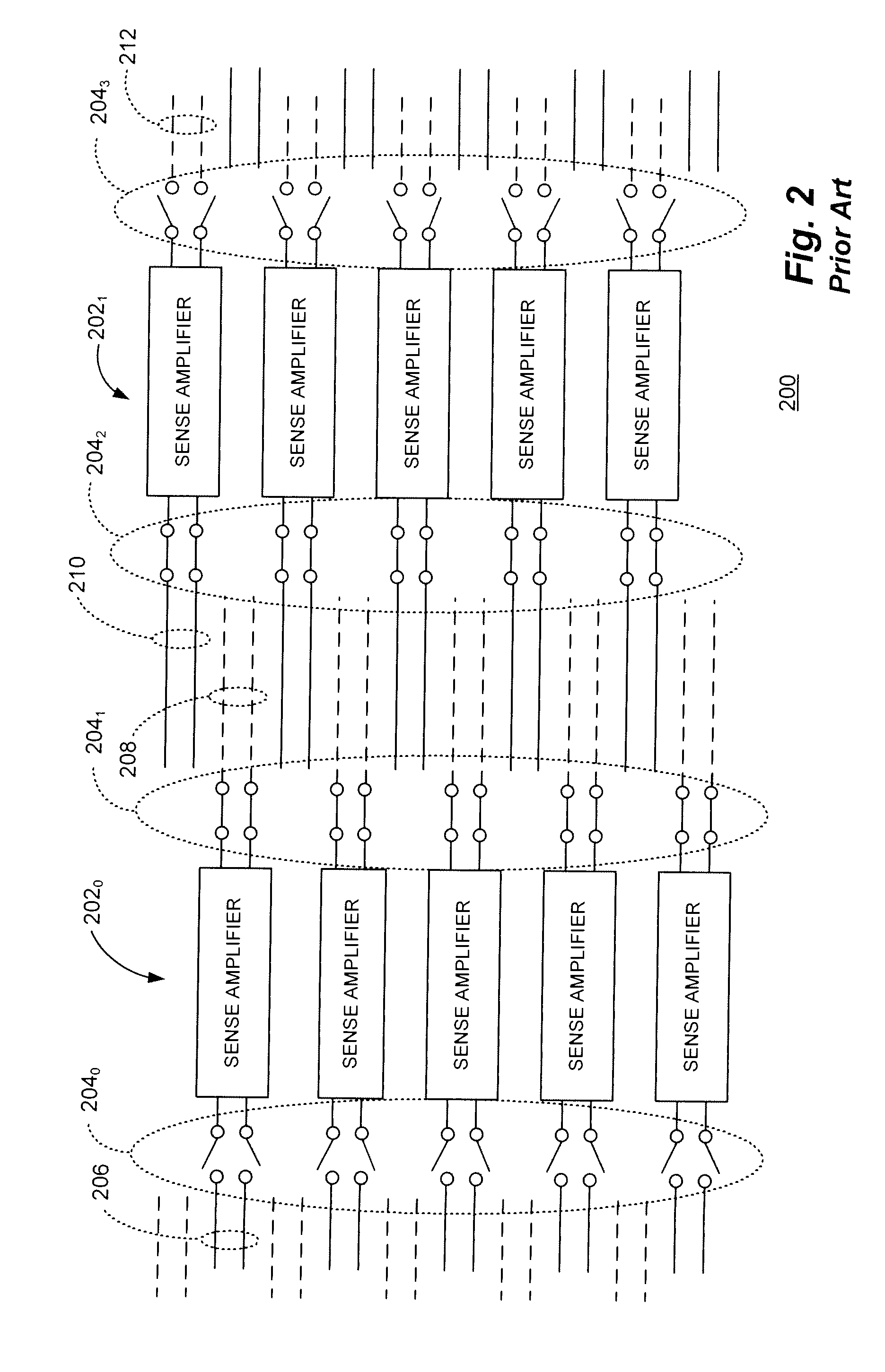
Figure 3
Abstract
Description
RELATED APPLICATION
[0001] The present application claims priority from, and is a divisional of, U.S. patent application Ser. No. 11 / 224,541 filed on Sep. 12, 2005. The disclosure of the foregoing U.S. Patent Application is specifically incorporated herein by this reference in its entirety and assigned to ProMOS Technologies PTE.LTD., Singapore, assignee of the present invention.BACKGROUND OF THE INVENTION
[0002] The present invention relates, in general, to the field of integrated circuit (IC) memory devices including dynamic random access memory (DRAM) devices and other integrated circuit devices incorporating embedded DRAM. More particularly, the present invention relates to a shielded bitline architecture for DRAM arrays.
[0003] Many types of DRAM based devices, or integrated circuits including embedded memory arrays, are currently available including extended data out (“EDO”), synchronous DRAM (“SDRAM”), double data rate (“DDR”), DDR3 DRAM and the like. Regardless of configurat...
Examples
Embodiment Construction
[0020] With reference now to FIG. 1, a portion of a representative folded bitline DRAM array 100 is shown in which the bitlines labeled BLB (bitline bar; e.g. BLB1 and BLB2) are available to act as reference inputs to the sense amplifier (not shown) for the bitlines labeled BL (e.g. BL1 and BL2) when a wordline (WL) is taken “high”.
[0021] Each of the memory cells of the DRAM array 100 comprise an N-channel access transistor 10211 through 10216 and 10221 through 10226 and an associated storage capacitor 10411 through 10416 and 10421 through 10426 respectively. Each of the transistors 102 has its drain terminal coupled to one of the corresponding complementary bitlines and its gate coupled to one of the wordlines WL1 through WL6. The source terminal of the transistors 102 is coupled one plate of the corresponding capacitor 104 which, in turn, has its other plate coupled to circuit ground (VSS) or a common plate line depending upon the particular memory technology employed.
[0022] As ...