
Metal-insulator-metal transformer and method for manufacturing the same
a technology of metal transformers and metal-insulators, applied in the field of inductance, can solve the problems of large size of coplanar transformers, serious impact on device reliability, and high cost, and achieve the effects of increasing the coupling coefficient of transformers, reducing the space between coils, and saving the chip area
Patent Information
- Authority / Receiving Office
- US · United States
- Patent Type
- Patents(United States)
- Current Assignee / Owner
- Publication Date
- 2008-04-29
Smart Images
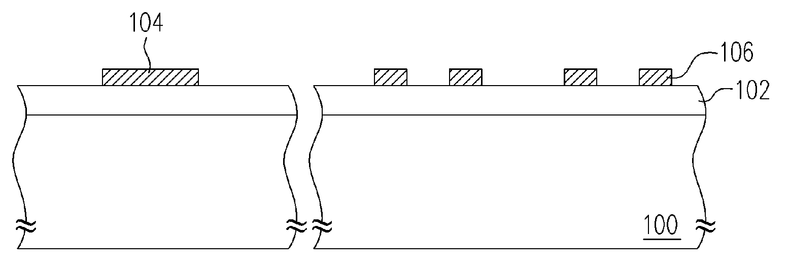
Figure 1 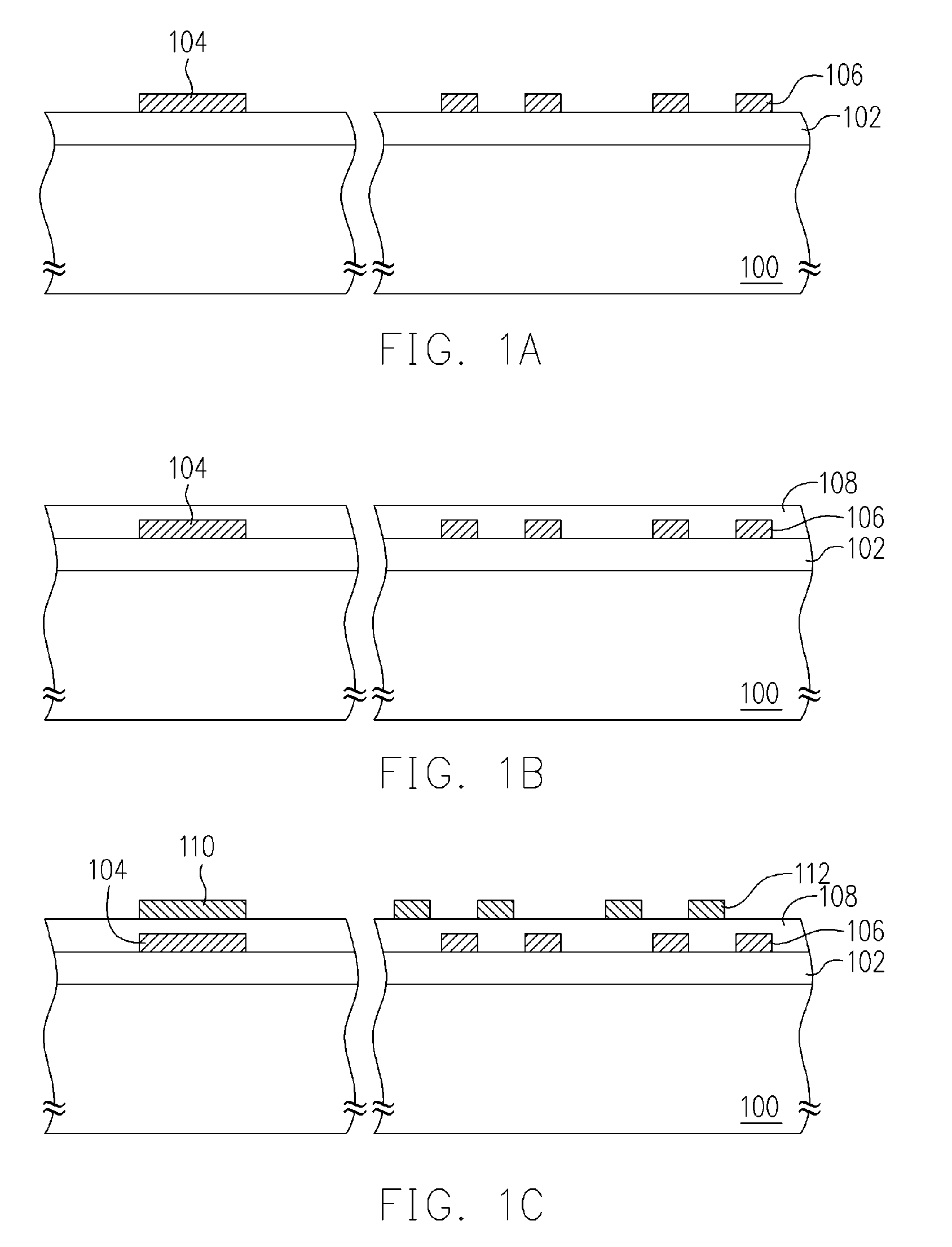
Figure 2 
Figure 3
Abstract
Description
BACKGROUND OF THE INVENTION
[0001] 1. Field of Invention
[0002] The present invention relates to an inductance and a manufacturing method thereof. More particularly, the present invention relates to a metal-insulating-metal transformer and the manufacturing method thereof.
[0003] 2. Description of Related Art
[0004] Currently, since the transformer possesses the advantages including high efficiency, no magnetic leakage and low noise, the transformer becomes one of the essential elements in the radio integrated circuit. Moreover, the transformer is widely used in many applications such as microwave and radio frequency circuit.
[0005] The transformer is composed of a core and two coils, primary coil and secondary coil. Generally, the core is used as a medium and two coils are wound around the core. While the alternating current is applied onto the primary coil, a magnetic flux which is perpendicular to the coils is generated within the core. According to the magnetic flux within the core, a vol...
Examples
Embodiment Construction
[0038]FIGS. 1A through 1C are cross-sectional views illustrating a method for manufacturing a metal-insulator-metal transformer according to a preferred embodiment of the invention.
[0039]As shown in FIG. 1A, a substrate 100 is provided. The substrate 100 possesses at least one dielectric layer 102 formed thereon. The dielectric layer 102 can be, for example but not limited to, made of silicon oxide, silicon nitride, the dielectric material with low dielectric constant or the other well known dielectric material. The method for forming the dielectric layer 102 comprises steps of performing a chemical vapor deposition process to deposit a dielectric layer (not shown) over the substrate 100 and then performing a planarizing process by using the chemical mechanical polishing. The dielectric layer 102 can be, for example, a complex layer having a multi-layered structure. Furthermore, on the substrate 100 and within the dielectric layer 102, there are several devices and metal interconnec...