
Semiconductor device and method of manufacturing semiconductor device
Patent Information
- Authority / Receiving Office
- US · United States
- Current Assignee / Owner
- Publication Date
- 2019-02-28
Smart Images
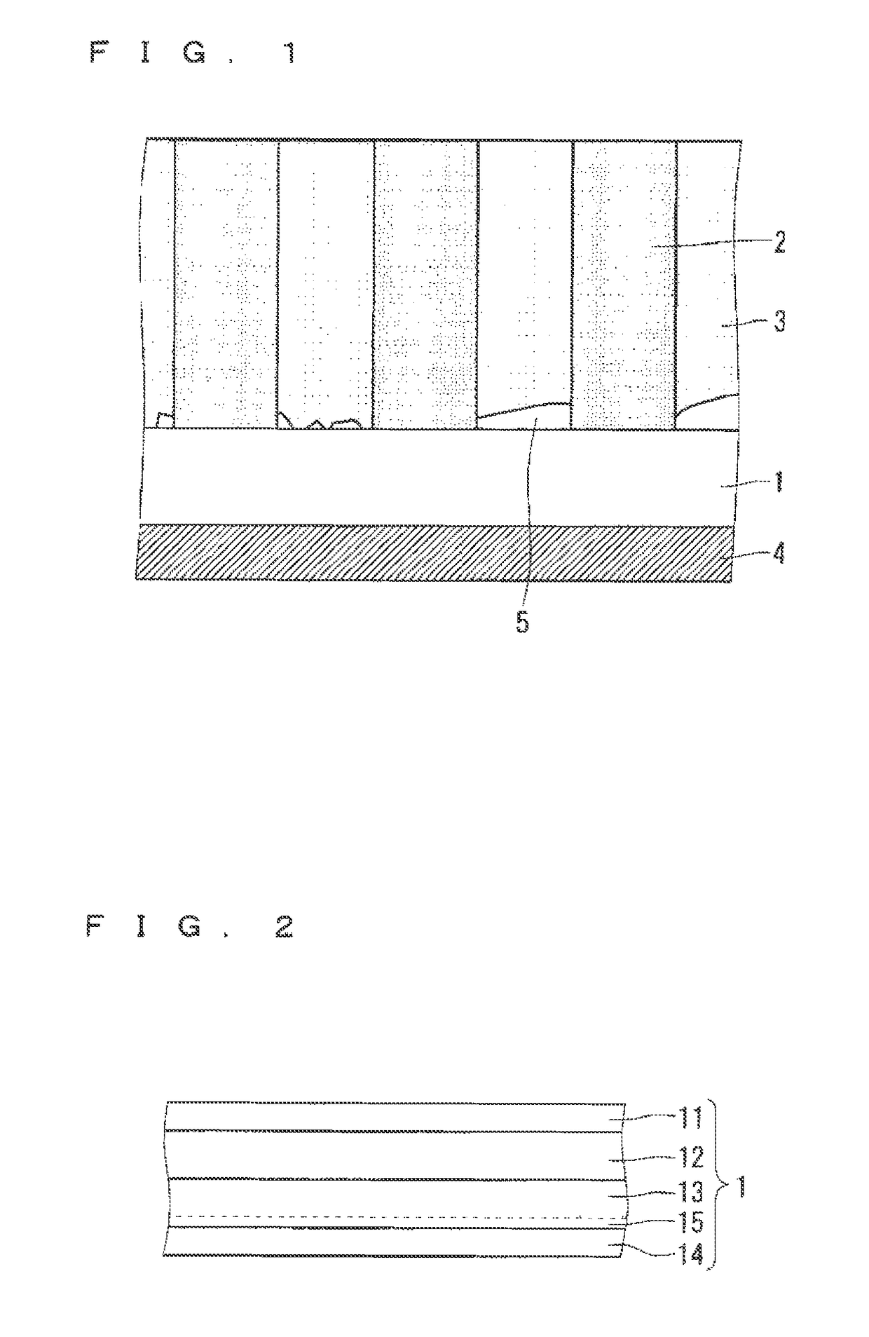
Figure 1 
Figure 2 
Figure 3
Abstract
Description
TECHNICAL FIELD
[0001] The present invention relates to a semiconductor device including a crystalline nitride layer, and a manufacturing method therefor.BACKGROUND ART
[0002] Nitrides such as gallium nitride (GaN), aluminum nitride (AlN), and aluminum gallium nitride (AlGaN) have a high dielectric breakdown electric field and a high carrier velocity, and hence application to a high-output and high-frequency electronic device or optical device is expected. However, there is a problem in that output characteristics are limited due to self-heat generation at die time of a high output operation.
[0003] As a countermeasure therefor, for example. Patent Document 1 discloses a semiconductor device including a diamond layer embedded in a hole provided in a bottom surface of a substrate, a single-crystal nitride layer provided on an upper surface side of the substrate, and a device layer provided thereon. Diamond has the highest thermal conductivity among substances and is excellent in heat dissi...
Examples
first embodiment
[0024]FIG. 1 is a cross-sectional view illustrating a configuration of a semiconductor device (group III nitride semiconductor device) according to a first embodiment of the present invention.
[0025]In a structure in which diamond is brought into contact with a crystalline nitride layer, there is a problem in that a crack of the crystalline nitride layer is generated due to di(Terence in thermal expansion coefficients between the diamond and the crystalline nitride layer. As will be apparent in the description below, the semiconductor device of FIG. 1 is capable of solving such a problem.
[0026]The semiconductor device of FIG. 1 includes a crystalline nitride layer 1, a structure 2 containing silicon (Si), a diamond layer 3, and a device layer 4. The structure 2 is selectively disposed on an upper surface (first main surface) of the crystalline nitride layer 1. The diamond layer 3 is disposed at least on a lateral portion of the structure 2, and a stress absorbing space 5 being a void...
second embodiments
[0059]FIG. 8 is a cross-sectional view illustrating a configuration of a semiconductor device according to a second embodiment of the present invention. In the description below, in the semiconductor device according to this second embodiment, components that are the same as or similar to diose of the first embodiment are denoted by the same reference symbols, and different components are mainly described.
[0060]Difference of the semiconductor device according to this second embodiment from the semiconductor device according to the first embodiment resides in that the structure 2 has a triangular shape in a cross-sectional view. With this, adjacent lateral surfaces of adjacent structures 2 are unparallel to each other. Specifically, in adjacent first structure 2 and second structure 2, a lateral surface close to the second structure 2 in a lateral surface of the first structure 2 and a lateral surface close to the first structure 2 in a lateral surface of the second structure 2 are u...
third embodiment
[0068]FIG. 9 is a cross-sectional view illustrating a configuration of a semiconductor device according to a third embodiment of the present invention. In the description below, in the semiconductor device according to this third embodiment, components that are the same as or similar to those of the first embodiment are denoted by the same reference symbols, and different components are mainly described.
[0069]In this third embodiment, a gate electrode 4a is included in the device layer 4. The gate electrode 4a is selectively disposed on the second main surface that is opposite to the First main surface of the crystalline nitride layer 1. Further, at least a part of the gate electrode 4a is positioned below the structure 2.
[0070]Here, heat generation occurs inside the crystalline nitride layer 1 above the gate electrode 4a. In view of this, in this third embodiment, al least a part of die gate electrode 4a is positioned below the structure 2, and hence die above-mentioned heat can be...