
Low noise op amp
a low-noise op amp and low-noise technology, applied in the field of amplifiers, can solve the problems of flicker noise improvement and over-all flicker noise of the circuit, and achieve the effects of reducing oxide thickness, low operating voltage, and reducing flicker nois
Patent Information
- Authority / Receiving Office
- US · United States
- Patent Type
- Patents(United States)
- Current Assignee / Owner
- Publication Date
- 2006-09-26
Smart Images
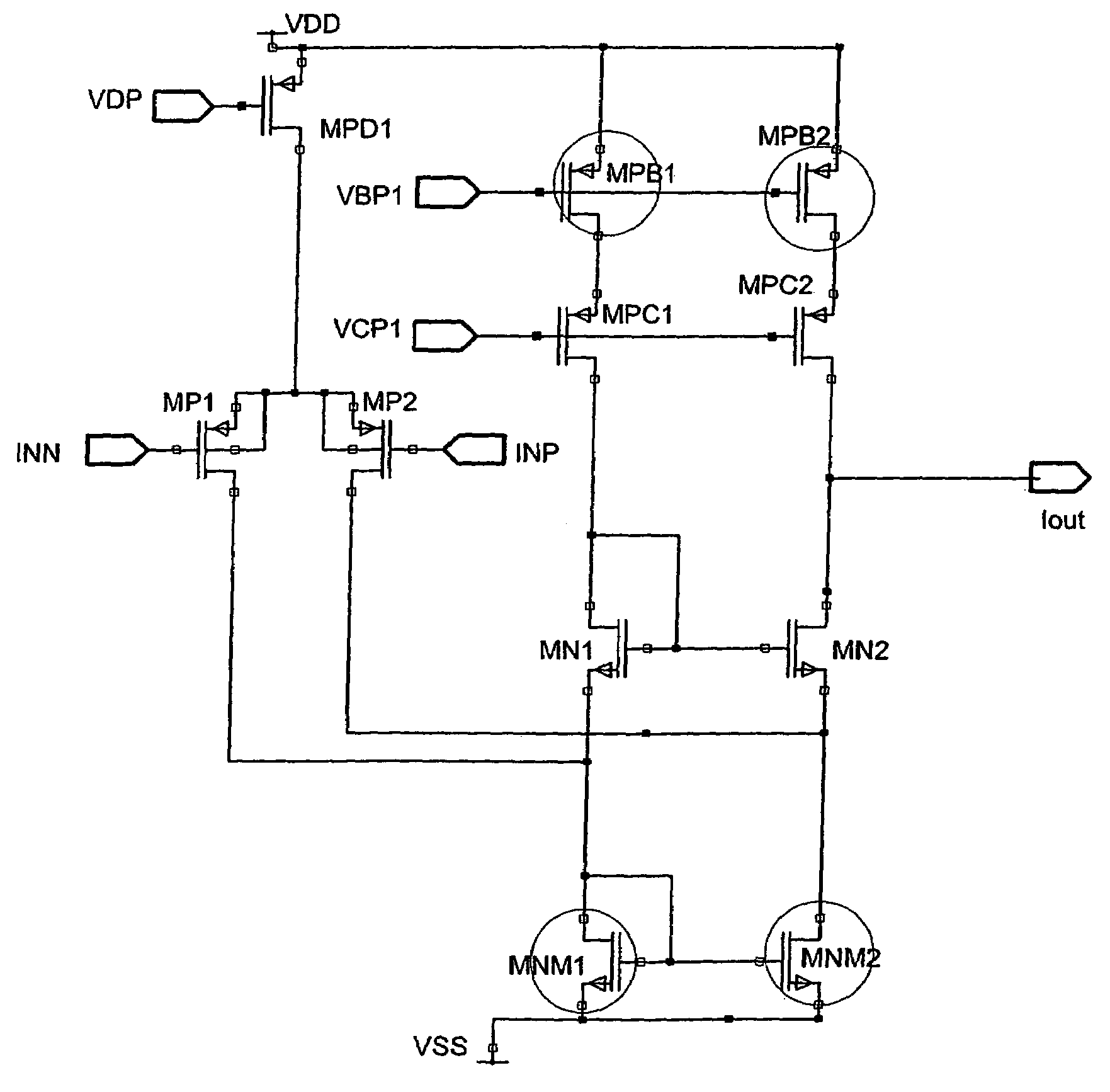
Figure 1 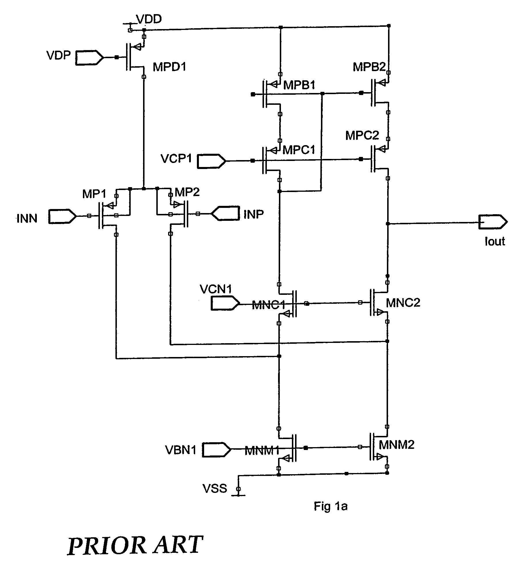
Figure 2 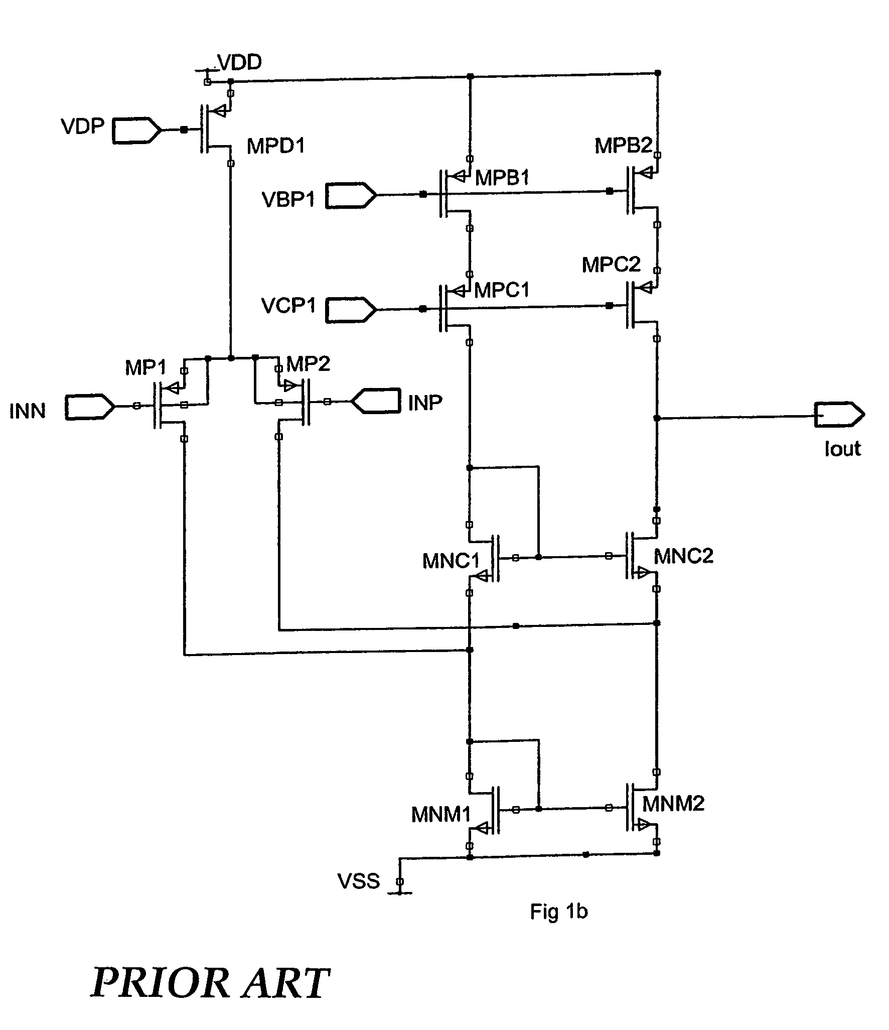
Figure 3
Abstract
Description
FIELD OF THE INVENTION
[0001] The present invention relates to amplifiers using metal oxide semiconductor based integrated circuits. The present invention is particularly but not exclusively related to audio application mixed signal chips.BACKGROUND OF THE INVENTION
[0002] Due to the increasing need for miniaturisation of portable devices such as MP3 players, mobile telephones and personal digital assistants, it has become increasingly important to implement both digital processing functions and related analogue, especially audio, processing functions on the same chip or integrated circuit—a so called mixed signal chip. For this reason the implementation of analogue functions on metal oxide semiconductor (MOS) based devices has become increasingly important.
[0003] A major problem with this technology however is that the digital and analogue circuits require different characteristics from the same semiconductor technology. Digital circuits are fastest and consume least power and chip area...
Examples
Embodiment Construction
[0037]Referring initially to FIG. 1b, a typical audio op amp design is shown which utilises a differential folded cascode arrangement. MOS based transistor devices MP1 and MP2 are input transistors. Signal current from MP2 passes through folded cascode device MNC2 to the output. Signal current from MP1 cannot pass through folded cascode device MNC1, since current I(MNC1) is equal to the constant current defined by the constant current source MPB1. The MP1 signal current therefore passes through the current mirror formed by MNM1, MNM2 and then through the cascode device MNC2 to the output. Thus MNM1, MNM2, MNC1, MNC2 act as a single ended to differential converter, as well as contributing a cascode function to increase output impedance of this transconductance stage. Transistors MPC1 and MPC2 serve as cascode devices to bias devices MPB1 and MPB2 to increase their effective output impedance, to maintain the high output impedance at Iout and also to improve power supply rejection.
[003...