
Method for manufacturing thin film transistor
a thin film transistor and manufacturing method technology, applied in the direction of basic electric elements, electrical apparatus, semiconductor devices, etc., can solve the problems of affecting the current characteristics of devices using polycrystalline silicon thin films, and affecting the electron migration of electrons. , to achieve the effect of improving current characteristics and high electron mobility
Patent Information
- Authority / Receiving Office
- US · United States
- Patent Type
- Patents(United States)
- Current Assignee / Owner
- Publication Date
- 2011-04-26
- Estimated Expiration
- Not applicable · inactive patent
Smart Images
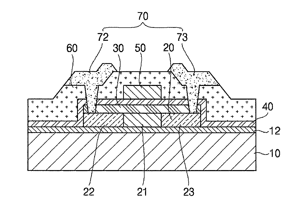
Figure 1 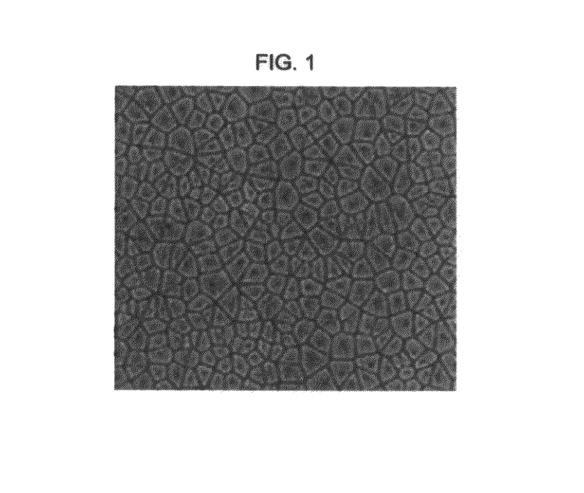
Figure 2 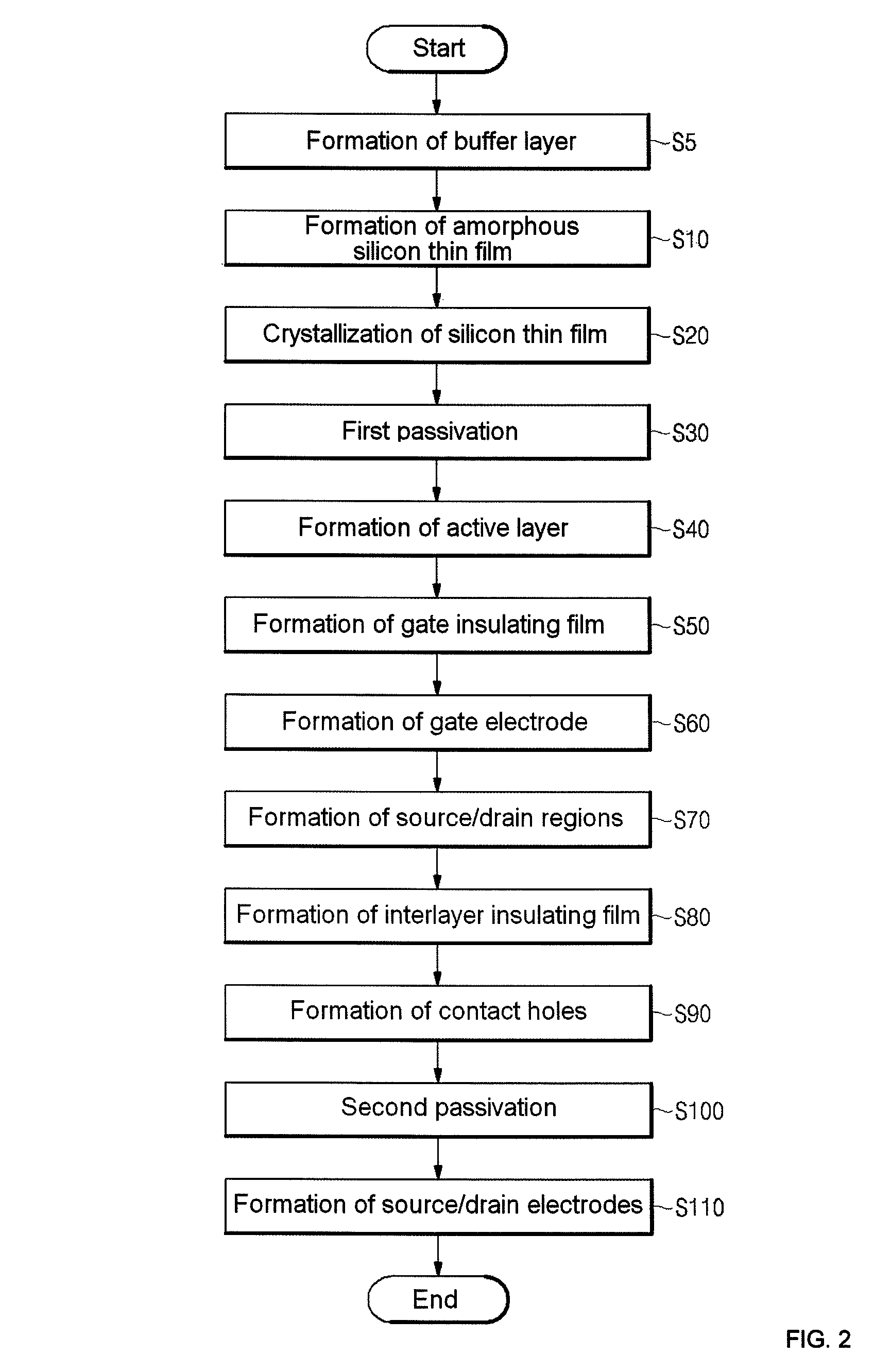
Figure 3
Abstract
Description
CROSS-REFERENCE TO RELATED APPLICATIONS
[0001] This application claims the benefit of Korean Application No. 10-2007-0140742, filed Dec. 28, 2007, and No. 10-2008-0033105, filed Apr. 10, 2008 in the Korean Intellectual Property Office, the disclosures of which are incorporated herein by reference.BACKGROUND OF THE INVENTION
[0002] 1. Field of the Invention
[0003] Aspects of the present invention relate to a method for manufacturing a thin film transistor with improved current characteristics and high electron mobility in which when an amorphous silicon thin film is crystallized into a polycrystalline silicon thin film by metal-induced crystallization, annealing conditions of the amorphous silicon thin film and the amount of a metal catalyst doped into the amorphous silicon thin film are optimized to reduce the regions of a metal silicide distributed at grain boundaries of the polycrystalline silicon thin film, and in which oxygen (O2) gas or water (H2O) vapor is supplied to form a passiva...
Examples
example 1
[0093]The amorphous silicon thin films were crystallized at different temperatures to form polycrystalline silicon thin films. To clearly observe the temperature-dependent crystallization of the amorphous silicon thin films, the annealing time was decreased with increasing annealing temperature. The annealing of the amorphous silicon thin films was performed under the following sets of temperature / time conditions: 600° C. / 150 minutes (Example 1a), 650° C. / 80 minutes (Example 1b), 700° C. / 20 minutes (Example 1c), 750° C. / 10 minutes (Example 1d), and 800° C. / 5 minutes (Example 1e). The metal catalyst was doped at the same concentration (2×10¹³ / cm2).
example 2
[0094]In this example, the amorphous silicon thin films were crystallized for different periods of time while maintaining the annealing temperature constant to form polycrystalline silicon thin films. Specifically, the amorphous silicon thin films were annealed at 700° C. for 5 minutes (Example 2a), 10 minutes (Example 2b), 20 minutes (Example 2c) and 40 minutes (Example 2d). The metal catalyst was doped at the same concentration (2×10¹³ / cm2).
example 3
[0095]In this example, the amorphous silicon thin films were crystallized by doping the metal catalyst at different concentrations while maintaining the annealing temperature and time constant. Specifically, the metal catalyst was doped at different concentrations: 5×10¹¹ / cm2 (Example 3a), 2×10¹² / cm2 (Example 3b), 2×10¹³ / cm2 (Example 3c), 6×10¹⁴ / cm2 (Example 3d) and 5×10¹⁵ / cm2 (Example 3e). The doped amorphous silicon thin films were annealed at the same temperature (750° C.) for the same period of time (5 minutes) to form polycrystalline silicon thin films.
[0096]The results obtained after the annealing of the amorphous silicon thin films under the different crystallization conditions in Examples 1-3 were evaluated as follows.
[0097]Each of the polycrystalline silicon thin films was etched. The morphology of grain boundaries of the etched thin film was observed. When a general polycrystalline silicon thin film is etched, a metal silicide present at grain boundaries of the polycrystal...