
Electrostatic discharge protection device
a protection device and electrostatic discharge technology, applied in the field of electrostatic discharge protection devices, can solve the problems of gate dielectric layer breakdown voltage, internal circuit gate dielectric damage, and other problems, to achieve the effect of improving the current characteristics of parasitic diodes
Patent Information
- Authority / Receiving Office
- US · United States
- Patent Type
- Patents(United States)
- Current Assignee / Owner
- Publication Date
- 2011-10-18
- Estimated Expiration
- Not applicable · inactive patent
Smart Images
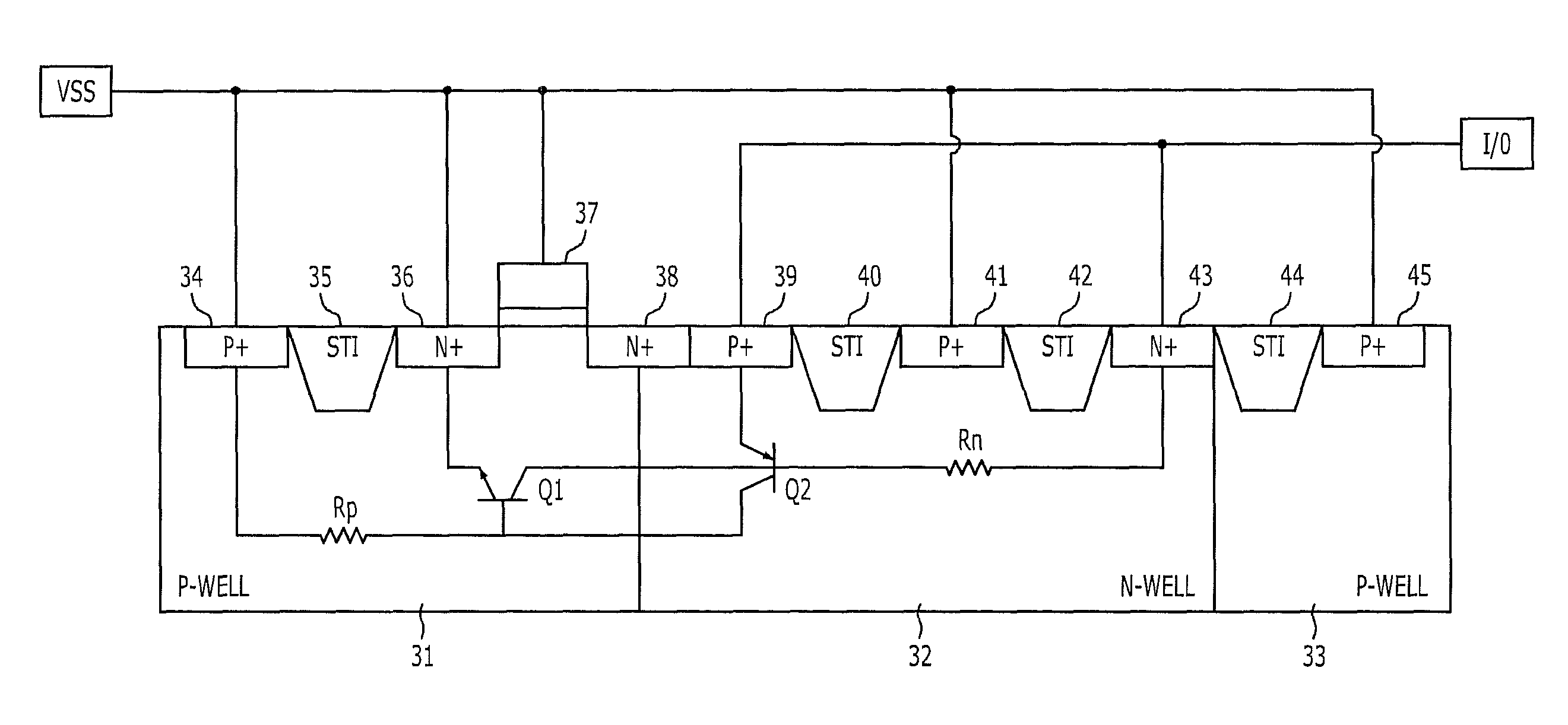
Figure 1 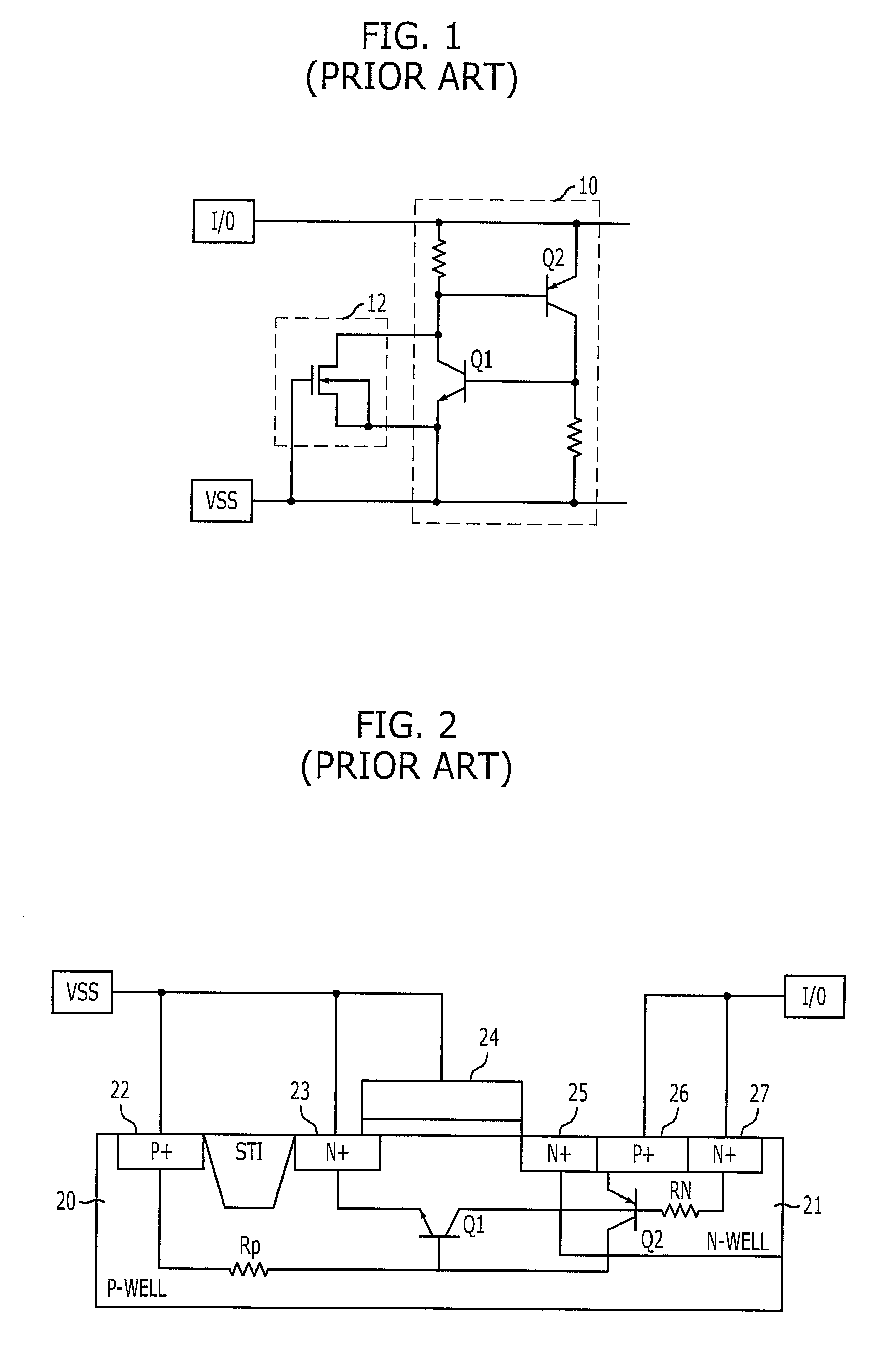
Figure 2 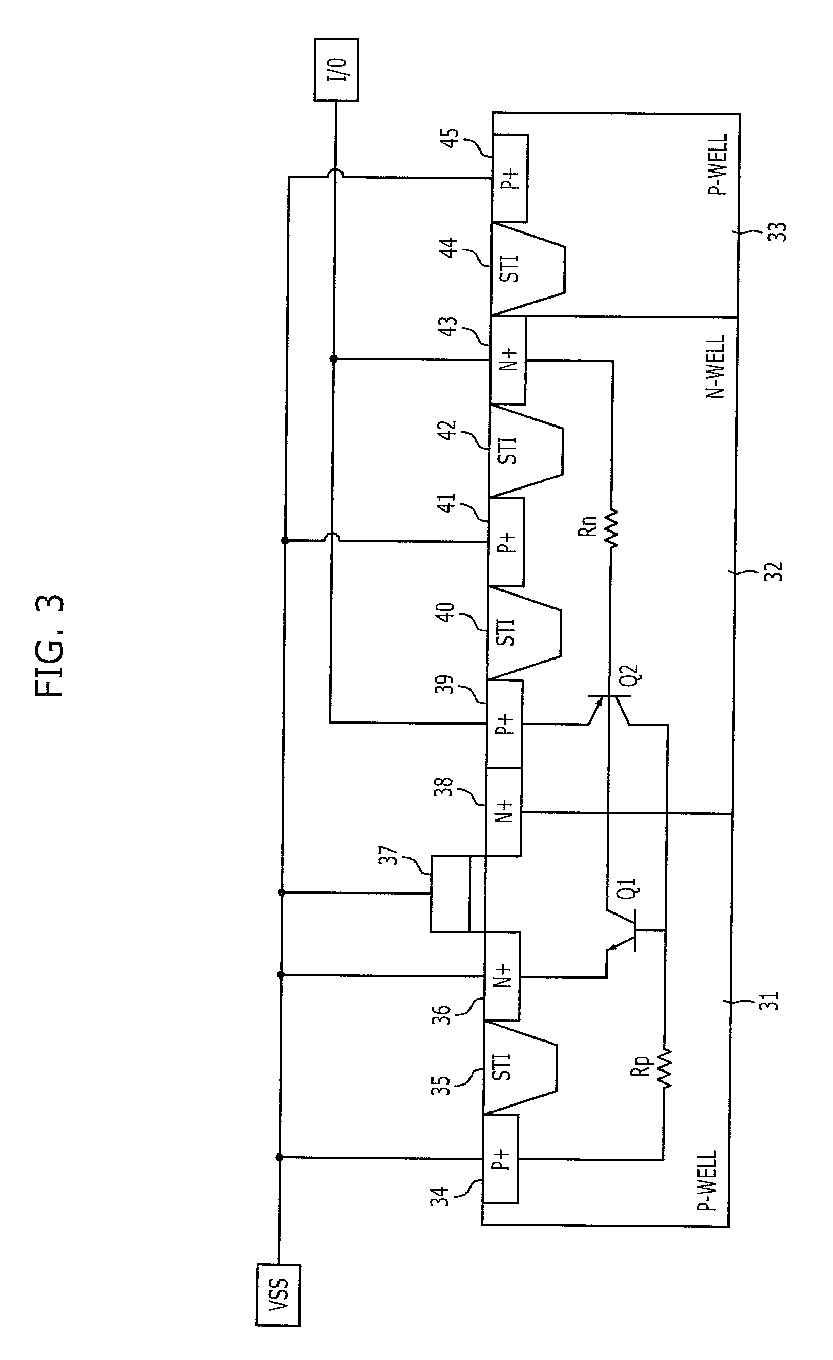
Figure 3
Abstract
Description
CROSS-REFERENCE TO RELATED APPLICATIONS
[0001] The present invention claims priority of Korean patent application number 10-2008-0049878, filed on May 28, 2008, the disclosure of which is incorporated by reference herein in its entirety.BACKGROUND OF THE INVENTION
[0002] The present invention relates to a semiconductor device, and more particularly, to an electrostatic discharge (ESD) protection device for protecting internal circuits from ESD.
[0003] ESD is the sudden electric current flowing between two insulating objects when placed under a large electric potentials caused by direct electrical contact.
[0004] When a high voltage caused by ESD flows into semiconductor devices, internal circuits may be damaged. Thus, most semiconductor devices include an ESD protection device between a pad and an internal circuit in order for protecting the internal circuit from being damaged.
[0005] As semiconductor devices are being operated at higher speeds and highly integrated, a low pin capacitance may...
Examples
Embodiment Construction
[0046]Other objects and advantages of the present invention can be understood by the following description, and become apparent with reference to the embodiments of the present invention.
[0047]FIG. 3 is a cross-sectional view of an ESD protection device in accordance with an embodiment of the present invention, and a circuit diagram of the ESD protection device is omitted to the extent that it is the same as the prior art. Referring to FIG. 3, the ESD protection device includes an N-well 32 between P-wells 31 and 33.
[0048]N-type impurity regions 36 and 38, and a gate 37 formed of an oxide layer and a poly layer are disposed in the P-well 31 to form an NMOS transistor. A P-type impurity region 34 is formed on the left side of the N-type impurity region 36, with a device isolation layer 35 being disposed between the P-type impurity region 34 and the N-type impurity region 36.
[0049]The N-type impurity region 38 and the P-type impurity region 39 are joined together in the N-well 32. A d...