

Method for forming grid medium layer and estimating its electrical parameter
A gate dielectric layer and electrical parameter technology, which is applied in the manufacture of circuits, electrical components, semiconductors/solid-state devices, etc., can solve problems such as the inability to evaluate the electrical parameters of the gate dielectric layer online, and achieve improved electrical stability and Reliability, cost savings, and the effect of reducing R&D cycles
- Summary
- Abstract
- Description
- Claims
- Application Information
AI Technical Summary
Problems solved by technology
Method used
Image

Examples
Embodiment Construction
[0021] In order to make the above objects, features and advantages of the present invention more comprehensible, specific implementations of the present invention will be described in detail below in conjunction with the accompanying drawings.
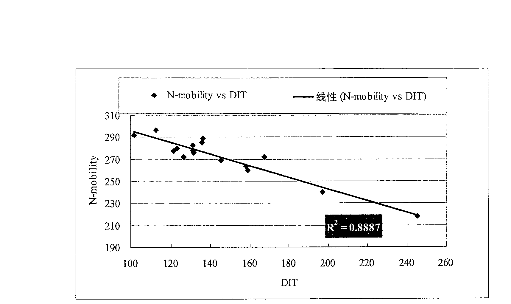
[0022] The gate dielectric layer plays a very important role as an insulating layer between the gate and the conductive channel of the substrate. The physical characteristic parameters of the gate dielectric layer will affect the formed device leakage current, turn-on voltage, carrier migration performance, and response speed The isoelectric parameter is also referred to as the electrical parameter of the gate dielectric layer in the present invention. Especially with the development of semiconductor technology to the technical node of 90nm and below, the thickness of the gate dielectric layer has been reduced to 5nm or even smaller. Controlling process parameters to form a high-quality gate dielectric layer is a problem that process pe...
PUM
 Abstract
Description
Claims
Application Information