

Touch panel and manufacturing method thereof
A technology of a touch panel and a manufacturing method, applied to instruments, electrical digital data processing, input/output process of data processing, etc., capable of solving the problem of inability to take into account the display characteristics of the protection function, reducing the light penetration of the touch panel 10, and unfavorable Solve problems such as display quality of touch display devices, achieve good optical quality and electrical quality
Patent Information
- Authority / Receiving Office
- CN · China
- Patent Type
- Applications(China)
- Current Assignee / Owner
- Publication Date
- 2010-04-28
- Estimated Expiration
- Not applicable · inactive patent
Smart Images
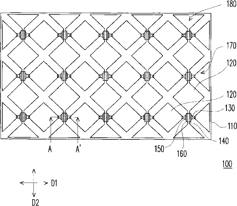
Figure 1 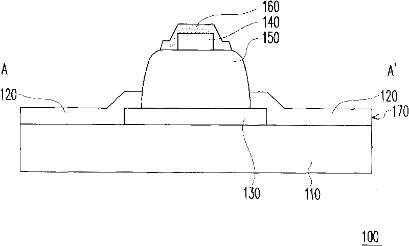
Figure 2 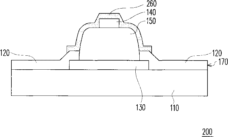
Figure 3
Abstract
Description
Technical field
[0001] The present invention relates to a touch panel, and in particular to a touch panel with good light penetration property.
Background technique
[0002] With the vigorous development of electronic technology and the popularization of wireless communication and networks, touch panels are often used as a human-machine interface between humans and smart devices to perform control. Most common touch panels are resistive touch panels and capacitive touch panels.
[0003] For the capacitive touch panel, the design of the capacitive touch panel is that a plurality of sensing pads are disposed on the substrate, and the touch action will change the capacitive effect between the sensing pads. Therefore, the capacitive touch panel can sense the touch position through such capacitive effect.
[0004] In order to protect the components in the capacitive touch panel, Chinese patent publication CN101334702 discloses a technology that utilizes a whole layer of scr...
Examples
Embodiment Construction
[0027] figure 1 A schematic partial top view of a touch panel according to an embodiment of the present invention is shown, and figure 2 for figure 1 The cross-sectional schematic diagram of the section line A-A'. Please also refer to figure 1 and figure 2 The touch panel 100 includes a substrate 110 , a plurality of sensing pads 120 , a plurality of first bridge lines 130 , a plurality of second bridge lines 140 , a plurality of first insulating patterns 150 and a plurality of second insulating patterns 160 .
[0028] The sensing pad 120 is disposed on the substrate 110 . The first bridge lines 130 are electrically connected in series with some of the sensing pads 120 to form a plurality of first sensing series 170 , and each first bridge line 130 extends along a first direction D1. Each second bridging line 140 extends along a second direction D2, wherein the first direction D1 is not parallel to the second direction D2. For example, the first direction D1 is perp...