
Asynchronous counter circuit and realizing method thereof
A counter and circuit technology, which is applied in the field of asynchronous counter circuits, can solve problems such as circuit instability, reset signal glitches, and flip-flops not being reset, so as to avoid reset instability, remove glitches, and improve reliability and stability. Effect
- Summary
- Abstract
- Description
- Claims
- Application Information
AI Technical Summary
Problems solved by technology
Method used
Image

Examples
Embodiment Construction
[0017] Specific embodiments of the present invention will be described in detail below in conjunction with the accompanying drawings.
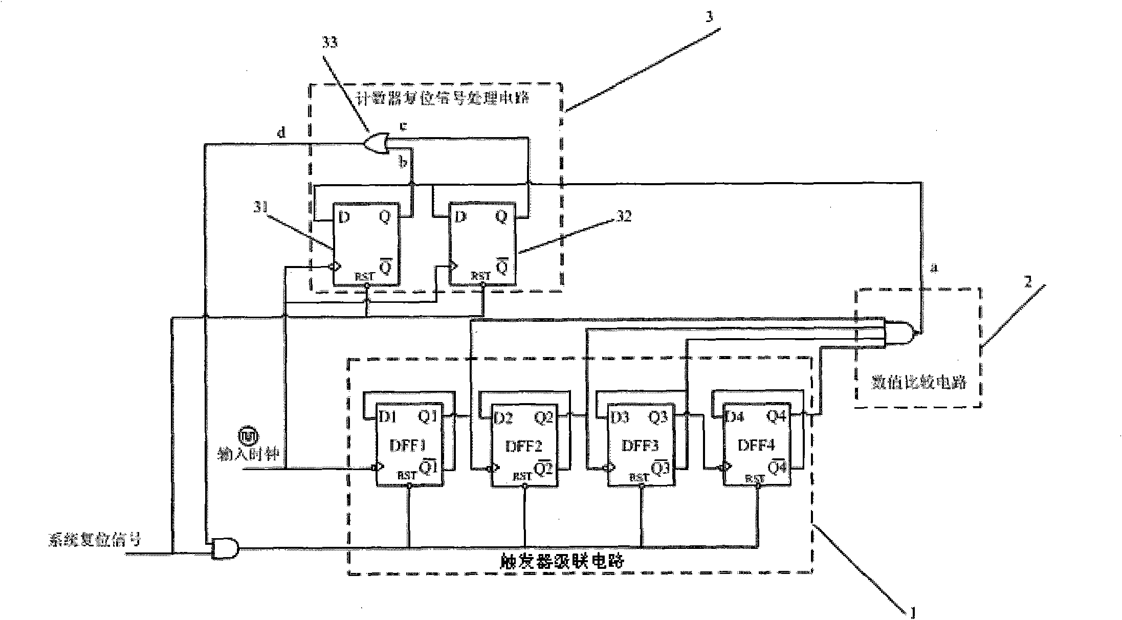
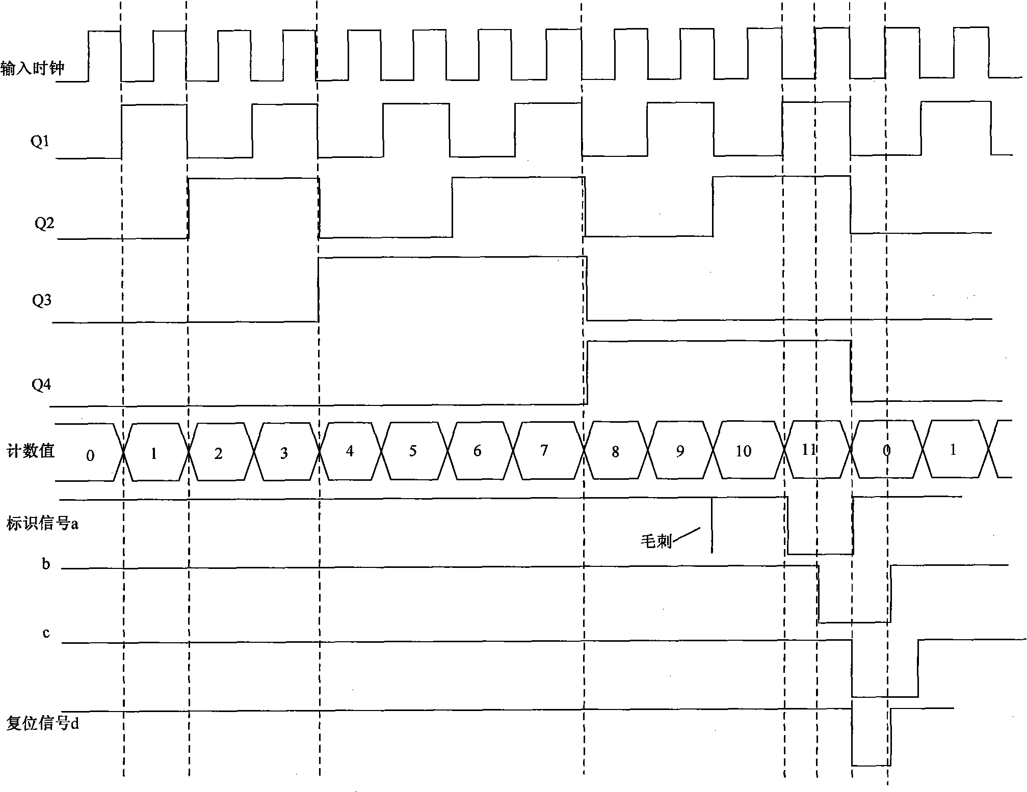
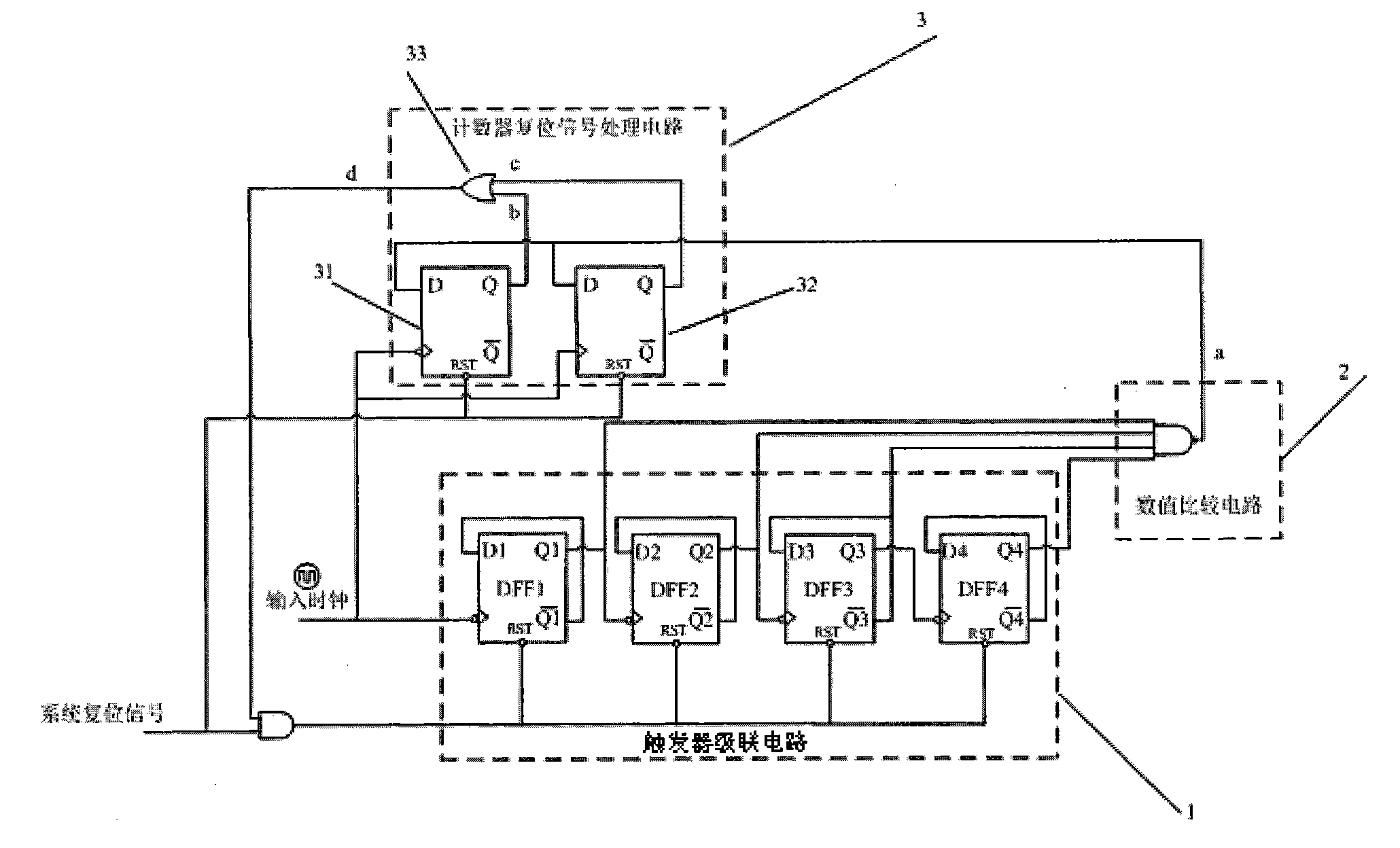
[0018] figure 1 It is a circuit structure diagram of a 12-ary asynchronous up-counter designed according to the circuit and method disclosed in the present invention.
[0019] In this specific implementation example, the flip-flop cascade circuit is composed of four falling-edge triggered D flip-flops DFF1-DFF4, and the D terminals of each flip-flop are respectively connected to their own inverting output terminals Q. The clock terminal of the first-stage flip-flop DFF1 is connected to the input clock, and the clock terminal of the subsequent-stage flip-flop is connected to the data output terminal of the previous-stage flip-flop. When the falling edge of the input clock arrives, DFF1 flips; when the Q terminal of the previous flip-flop flips from 1 to 0, the input of the next flip-flop flips.
[0020] The value comparison circuit is compose...
PUM
 Abstract
Description
Claims
Application Information