Analog accumulator capable of implementing time delay integration (TDI) function inside complementary metal-oxide semiconductor (CMOS) image sensor

An image sensor, accumulator technology, applied in the field of analog accumulators

Inactive Publication Date: 2012-07-18
TIANJIN UNIV
View PDF3 Cites 22 Cited by
  • Summary
  • Abstract
  • Description
  • Claims
  • Application Information

AI Technical Summary

Problems solved by technology

However, there is no suitable analog accumulator circuit in the pr...

Method used


Image

  • Analog accumulator capable of implementing time delay integration (TDI) function inside complementary metal-oxide semiconductor (CMOS) image sensor
  • Analog accumulator capable of implementing time delay integration (TDI) function inside complementary metal-oxide semiconductor (CMOS) image sensor
  • Analog accumulator capable of implementing time delay integration (TDI) function inside complementary metal-oxide semiconductor (CMOS) image sensor

Examples


Embodiment Construction

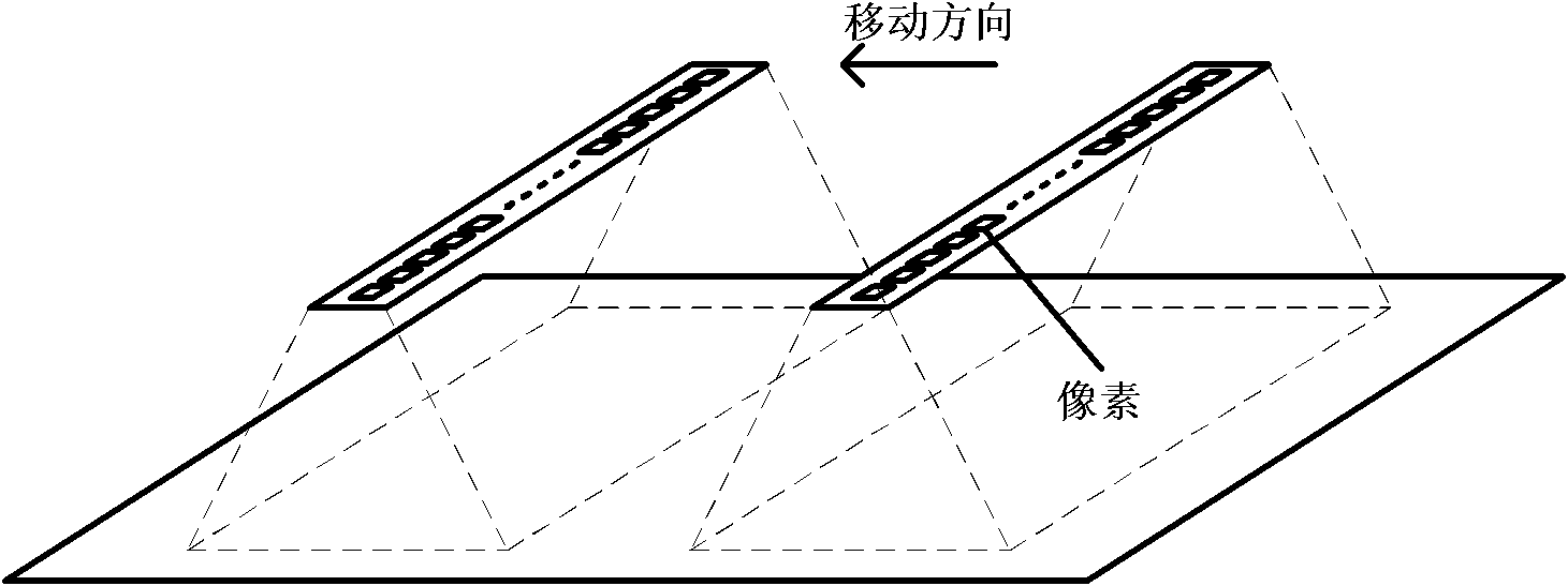
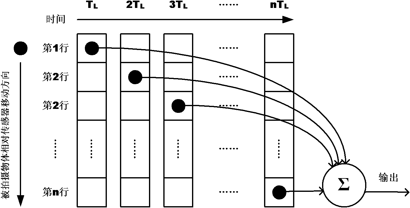
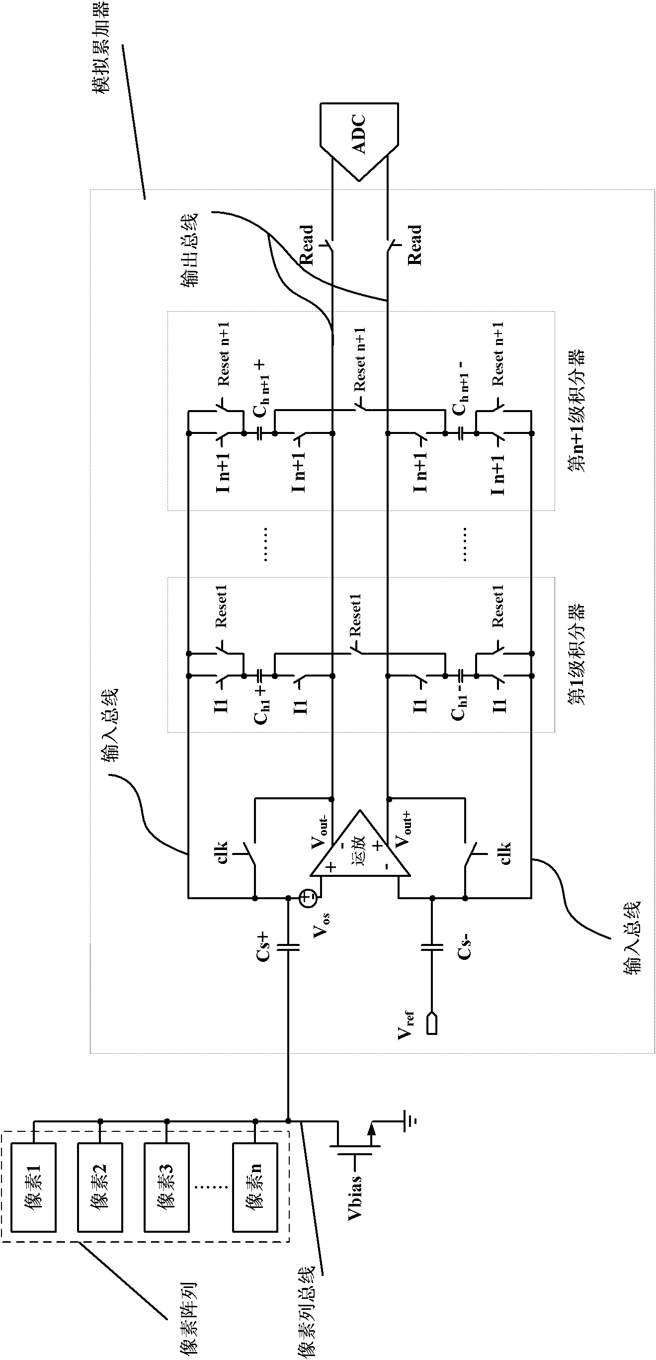
[0030] The circuit diagram of the analog accumulator reference image 3 , which mainly includes: sampling capacitor Cs, fully differential operational amplifier, two input buses, two output buses, n+1 sets of integrators, and the voltage source Vos is used to represent the input offset voltage of the operational amplifier. The CMOS-TDI image sensor adopts a drum-type exposure with an oversampling rate of (n+1) / n to realize the synchronization of exposure of different rows of pixels to the same object. The so-called drum exposure with an oversampling rate of (n+1) / n means that within one exposure period, the exposure is started successively from the pixels in the first row to the pixels in the nth row, and then the first row is added to the exposure start, so that in one exposure period The inner n rows of pixels will output n+1 data. The corresponding relationship between n rows of pixels in the pixel array and n+1 sets of integrators in the accumulator is as follows Figure...


PUM


Abstract

The invention relates to the design field of analog integrated circuits. The technical scheme includes that an analog accumulator capable of implementing a TDI function inside a CMOS image sensor comprises two differential sample capacitors Cs+ and Cs-, fully differential operation, two input buses, two output buses, a n+1 group integrator, the CMOS-TID image sensor adopts roll exposure with an over-sampling rate of (n+1)/n, left electrode plates of sample capacitors Cs+ and Cs- are respectively connected with an array bus of a pixel array and a reference voltage Vref, and right electrode plates of sample capacitors Cs+ and Cs- are respectively connected with a positive input end and a negative input end of the fully differential operation, so that the CMOS image sensor can perform the TID function well and the application range of the TDI technology is extended. The analog accumulator is mainly applied to design and manufacture of semiconductor image sensors.

Description

technical field [0001] The invention relates to the field of analog integrated circuit design, in particular to an analog accumulator for realizing TDI function inside a CMOS image sensor. Background technique [0002] The image sensor can convert the optical signal obtained by the lens into an electrical signal that is easy to store, transmit and process. Image sensors can be divided into area array type and line array type according to the working method. The working principle of the area array image sensor is to shoot an object with a pixel array arranged in a two-dimensional array to obtain two-dimensional image information, while the working principle of the line array image sensor is to use a pixel array arranged in a one-dimensional line array The two-dimensional image information is obtained by scanning and shooting the object, and the working method of the line array image sensor can be referred to figure 1 . Linear image sensors are widely used in many fields su...

Claims


Application Information

Patent Timeline
IPC IPC(8): H04N5/365H04N5/3745
Inventor 姚素英聂凯明徐江涛高静史再峰王彬徐新楠
Owner TIANJIN UNIV
Why Eureka
Try Eureka