

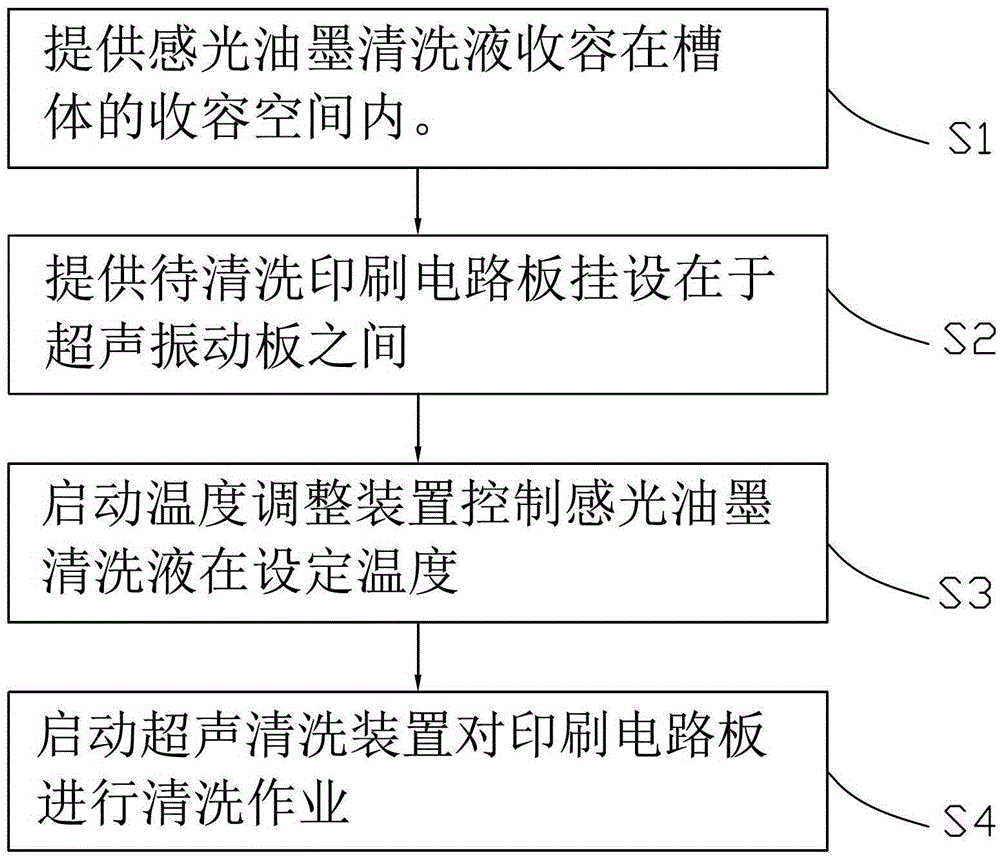
Printed circuit board processing technology and processing equipment
A technology for printed circuit boards and processing equipment, applied in the secondary treatment of printed circuits, cleaning/polishing of conductive patterns, etc., can solve the problems of low efficiency of heavy work, incomplete cleaning of residues, etc., achieve the best removal effect, and completely remove photosensitive ink , Improve the effect of working environment temperature
- Summary
- Abstract
- Description
- Claims
- Application Information
AI Technical Summary
Problems solved by technology
Method used
Image

Examples
Embodiment Construction
[0026] The present invention will be described in detail below in conjunction with the accompanying drawings.
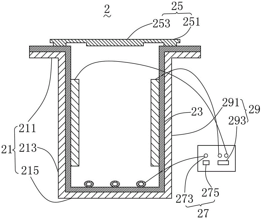
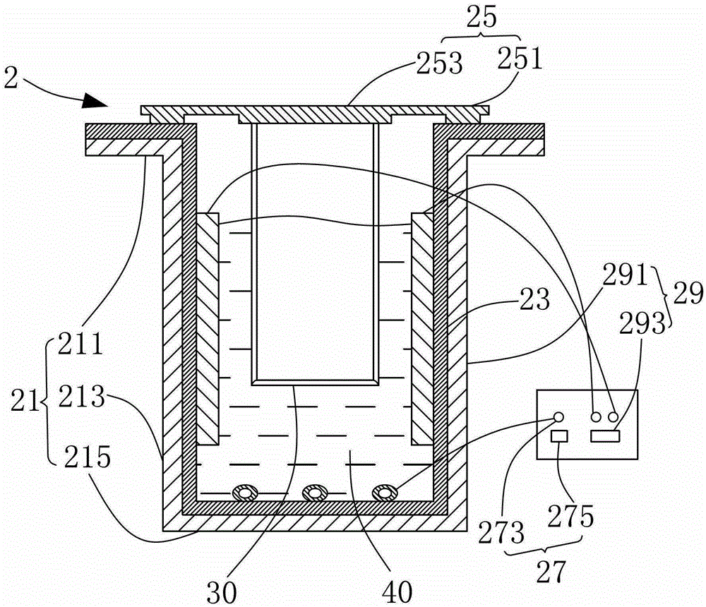
[0027] see figure 1 , is a schematic diagram of the side structure of a printed circuit board processing equipment disclosed in the present invention. The printed circuit board processing equipment 2 is used in the printed circuit board processing technology to completely remove and clean the photosensitive ink. The printed circuit board processing equipment 2 includes a tank body 21 , an anti-corrosion layer 23 , a support frame 25 , a temperature adjustment device 27 and an ultrasonic cleaning device 29 .
[0028] The tank body 21 includes a top edge 211 , a side wall 213 and a bottom wall 215 . The side wall 213 cooperates with the bottom wall 215 to form an opening receiving space, and the bottom wall 215 is connected to one end of the side wall 213 and closed to enclose it. The top edge 211 is an extension portion extending from the other edge of the side wal...
PUM
 Abstract
Description
Claims
Application Information