A display substrate and display device

A display and substrate technology, applied in static indicators, nonlinear optics, optics, etc., can solve problems such as uneven thickness of PI film, bad PI film mura, bad PI film, etc., to avoid PI film Poor layer, complete PI film layer, and consistent thickness

Active Publication Date: 2016-08-24
BOE TECH GRP CO LTD +1
View PDF7 Cites 0 Cited by
  • Summary
  • Abstract
  • Description
  • Claims
  • Application Information

AI Technical Summary

Problems solved by technology

When the PI liquid flows to the vicinity of the conductive sheet 500, the PI liquid will flow along the slit between the conductive sheets 500, and in a short time, the PI liquid forms a ring-shaped halo structure around the conductive sheet 500, and the conductive sheet 500 is close to the common There will be no PI liquid phenomenon near one side of the electrode line 300, and the thickness of the ring-shaped PI film layer around the conductive sheet 500 is also significantly greater than the thickness of the PI film layer near the middle part of the AA area. On the one hand, the AA area is close to the conductive layer. The missing problem of the PI film layer of the sheet 500, on the other hand, leads to the problem of uneven thickness of the PI film layer, resulting in defective PI film layer, also known as PI film layer mura defect

Method used


Image

  • A display substrate and display device
  • A display substrate and display device
  • A display substrate and display device

Examples


Embodiment Construction

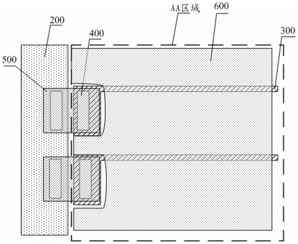
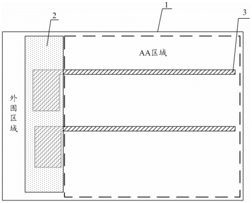
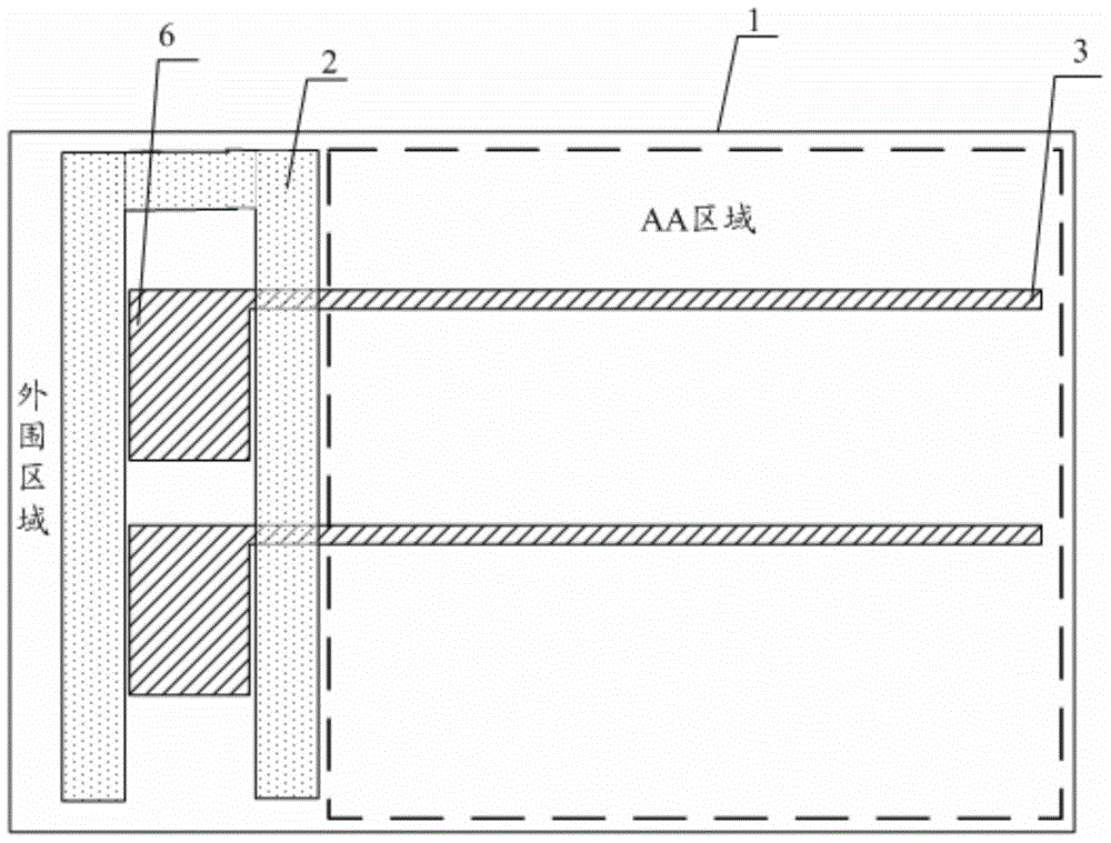
[0038] An embodiment of the present invention provides a display substrate and a display device. By extending the common electrode line of the display substrate located in the display area to the peripheral area, it is connected to the peripheral common electrode in the peripheral area, and the connection area is located in the peripheral area to avoid When the display area is sprayed with PI liquid, the PI film layer formed by the PI liquid is poor due to the slits between the multiple independent connection areas of the display area.

[0039] The present invention proposes that the common electrode lines are arranged on the same layer as the gate lines or data lines, and the common electrode lines are separated from each other in the display area, and it is necessary to electrically connect the common electrode lines in the display area or the peripheral area. Furthermore, it is proposed in view of the problem in the prior art that the common electrode lines are electrically ...


PUM


Abstract

The invention discloses a substrate for display and a display device. The problem that when PI liquid is sprayed on a display area, a PI film formed by the PI liquid is bad due to slits among a plurality of independent connecting areas of the display area is solved. The substrate for display comprises a lining substrate body, a peripheral common electrode and a plurality of common electrode lines, the peripheral common electrode is located in the peripheral area of the lining substrate body and extends in the first direction, the common electrode lines are located in the display area of the lining substrate body and at least extend to the area where the peripheral common electrode is located in the second direction crossing with the first direction, and the peripheral common electrode and the common electrode lines are arranged on different layers. The peripheral common electrode and the common electrode lines are insulated in the crossing area, and are connected in the peripheral area in a via hole bridging mode.

Description

technical field [0001] The invention relates to the technical field of liquid crystal display, in particular to a display substrate and a display device. Background technique [0002] In the field of display technology, wide viewing angles, high image quality and fast response speed have become urgent requirements for display devices. Currently, Advanced Super Dimension Switch (ADVanced Super Dimension Switch, ADSDS, ADS for short), and In-Plane Switching (IPS) type, or Vertical Alignment-In-Plane Switching (Vertical Aligment-In-Plane Switching, VA -IPS) liquid crystal display and other technologies, which have the characteristics of wide viewing angle, high image quality and fast response speed, have attracted much attention. [0003] In addition, the pursuit of high yield rate is also the goal that manufacturers have been pursuing. There are many factors that affect the product yield rate. For example, in the thin film transistor liquid crystal display (Thin Film Transis...

Claims


Application Information

Patent Timeline
Patent Type & Authority Patents(China)
IPC IPC(8): G02F1/133G02F1/1333G02F1/1343
Inventor 冯玉春陈曦王东亮王瑞瑞王守坤郭会斌
Owner BOE TECH GRP CO LTD
Why Eureka
Try Eureka