Organic electroluminescence device and display device

An electroluminescent device and luminescent technology, which is applied in the direction of organic semiconductor devices, electric solid devices, electrical components, etc., can solve the problems of small switching ratio, affecting screen display, increasing, etc., and achieve the goal of preventing impact and protecting performance Effect

Inactive Publication Date: 2015-01-21
BOE TECH GRP CO LTD
View PDF7 Cites 12 Cited by
  • Summary
  • Abstract
  • Description
  • Claims
  • Application Information

AI Technical Summary

Problems solved by technology

After the oxide thin film transistor in the OLED device is irradiated by ultraviolet light, the valence band electrons and forbidden band defects in the semiconductor layer can make the concentratedly captured electrons easily absorb energy and jump to the conduction band, thereby generating photogenerated electron-hole pairs, and finally Vth (threshold voltage) drifts, SS (subthreshold swing) increases, and the switching ratio becomes smaller, which in turn affects the entire OLED device and seriously affects the display of the screen

Method used


Image

  • Organic electroluminescence device and display device
  • Organic electroluminescence device and display device
  • Organic electroluminescence device and display device

Examples


Embodiment 1

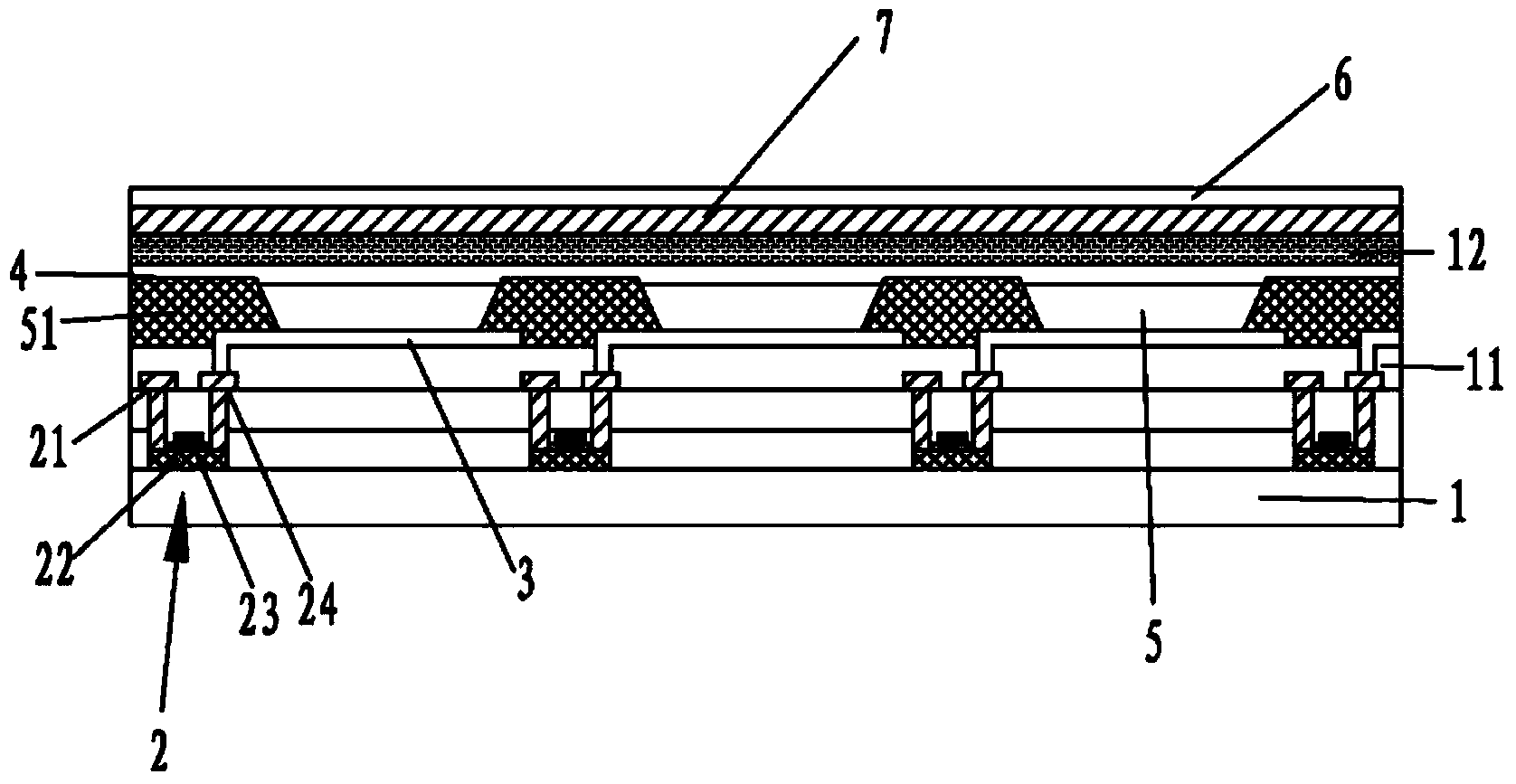
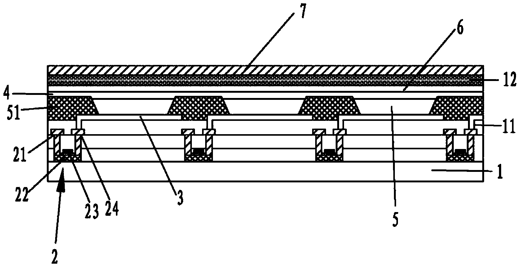
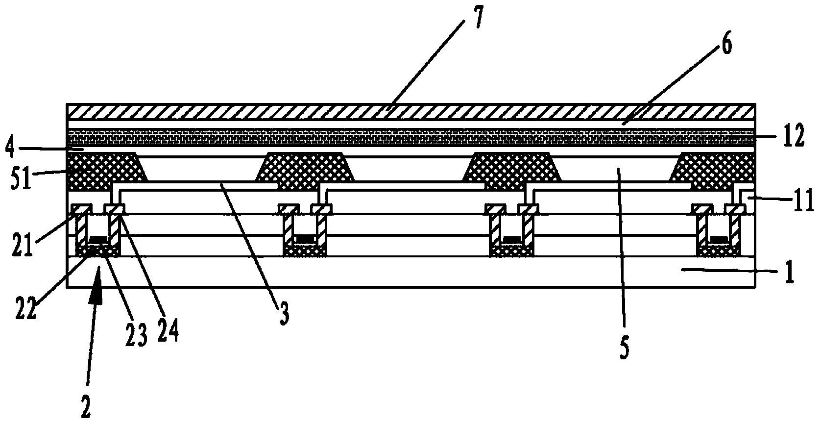
[0025] Such as figure 1 As shown, the embodiment of the organic electroluminescent device of the present invention includes a substrate 1, a thin film transistor 2, an anode 3, a cathode 4, and an organic light-emitting layer 5 for emitting light between the anode 3 and the cathode 4. The organic light-emitting layer The light emitting side of 5 is provided with a shielding layer 6 for shielding ultraviolet light.

[0026] In an embodiment of the organic electroluminescent device of the present invention, the thin film transistor 2 includes a source 21 , an active layer 22 , a gate 23 and a drain 24 .

[0027] In an embodiment of the organic electroluminescent device of the present invention, the anode 3 is arranged between the organic light-emitting layer 5 and the substrate 1, a first passivation layer 11 is arranged between the anode 3 and the substrate 1, and the outer side of the cathode 4 is arranged The second passivation layer 12 , the film layer 7 is arranged on the ...

Embodiment 2

[0030] combine figure 2 As shown, the difference between the embodiment of the organic electroluminescence device of the present invention and the first embodiment is that the shielding layer 6 is disposed between the second passivation layer 12 and the cathode 4 .

Embodiment 3

[0032] combine image 3 As shown, the difference between the embodiment of the organic electroluminescent device of the present invention and the first embodiment is that the blocking layer 6 is disposed between the thin film layer 7 and the second passivation layer 12 .


PUM


Abstract

The invention discloses an organic electroluminescence device and a display device. The organic electroluminescence device comprises a substrate, a thin film transistor, an anode, a cathode and an organic light-emitting layer used for emitting light. The organic light-emitting layer is located between the anode and the cathode. The light-emitting side of the organic light-emitting layer is provided with a shielding layer used for shielding ultraviolet. The display device comprises the organic electroluminescence device. According to the technical scheme, the shielding layer for shielding the ultraviolet is arranged inside the organic electroluminescence device to prevent ultraviolet from affecting properties of material of the organic light-emitting layer or the thin film transistor, and then the properties of the whole organic electroluminescence device are protected.

Description

technical field [0001] The invention relates to the field of electroluminescence, in particular to an organic electroluminescence device and a display device. Background technique [0002] Organic electroluminescent display (OLED) devices have the advantages of low energy consumption, high brightness, fast response time, wide viewing angle, light weight, etc., and have been widely used in mobile communication terminals, personal digital assistants (PDAs), and handheld computers recently. Compared with LCDs, the process of manufacturing OLED devices is relatively simple, which can reduce production costs. The core component of an organic electroluminescent display device is an organic electroluminescent device. [0003] The organic light-emitting material layer or TFT (Thin Film Transistor, Thin Film Transistor) in the OLED device will undergo property changes or performance degradation after being irradiated by external ultraviolet rays. After the oxide thin film transisto...

Claims


Application Information

Patent Timeline
Patent Type & Authority Applications(China)
IPC IPC(8): H01L51/50H01L51/52H01L27/32
CPCH10K59/00H10K50/00H10K50/86H10K59/126H10K59/122H10K2102/00H10K50/844
Inventor 程鸿飞张玉欣
Owner BOE TECH GRP CO LTD
Why Eureka
Try Eureka