A display device and its driving method

A technology for display devices and display panels, which is applied to identification devices, static indicators, optics, etc., can solve the problems that the organic light-emitting layer cannot achieve a smaller area, a large pixel area, and cannot meet the requirements of high display resolution products.

Active Publication Date: 2018-02-27
BOE TECH GRP CO LTD
View PDF5 Cites 0 Cited by
  • Summary
  • Abstract
  • Description
  • Claims
  • Application Information

AI Technical Summary

Problems solved by technology

[0004] However, since the organic light-emitting layer of OLED is generally prepared by mask evaporation method, that is, the organic light-emitting layer is formed through a mask, and due to the limitation of the mask, the organic light-emitting layer cannot achieve a smaller area, and the pixel area Larger, which in turn makes it unable to meet the requirements for high display resolution products

Method used


Image

  • A display device and its driving method
  • A display device and its driving method
  • A display device and its driving method

Examples


Embodiment Construction

[0032] The following will clearly and completely describe the technical solutions in the embodiments of the present invention with reference to the accompanying drawings in the embodiments of the present invention. Obviously, the described embodiments are only some, not all, embodiments of the present invention. Based on the embodiments of the present invention, all other embodiments obtained by persons of ordinary skill in the art without making creative efforts belong to the protection scope of the present invention.

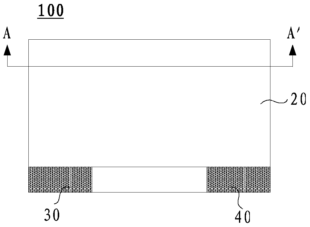
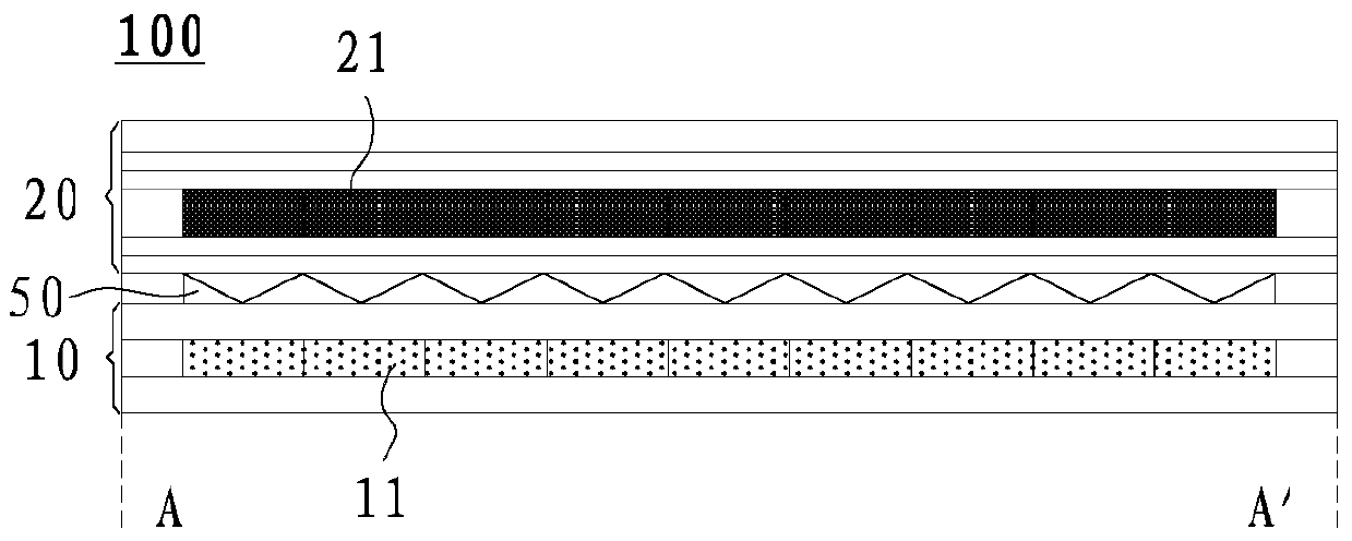
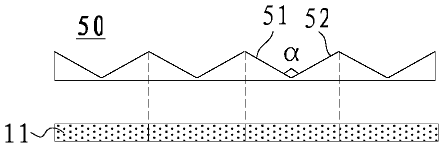
[0033] An embodiment of the present invention provides a display device 100, such as Figure 1-Figure 2 As shown, it includes a display panel 10, a first driving module 30, a second driving module 40, and an optical modulator 20 located on the light-emitting side of the display panel 10, and a plurality of prism structures are formed between the display panel 10 and the optical modulator 20, figure 2 The middle prism layer 50 is formed with a plurality of pri...


PUM

PropertyMeasurementUnit
thicknessaaaaaaaaaa
transmittivityaaaaaaaaaa
reflectanceaaaaaaaaaa

Abstract

The invention provides a display device and a driving method thereof, relates to the field of display technology, and solves the problem that the existing display panels are difficult to achieve high resolution. A display device, comprising a display panel, a first drive module, a second drive module, and an optical modulator located on the light-emitting side of the display panel, a plurality of prism structures are formed between the display panel and the light modulator, and the pixels include n dummy pixels, The light modulation unit includes: n light modulation regions respectively corresponding to virtual pixels; one frame picture includes n sub-frame pictures; the first driving module is used to drive the display panel to sequentially display n consecutive sub-frame pictures in one frame picture; The second drive module is used to drive the n light modulation areas of the light modulation unit to be light-transmitting areas in the n sub-frame pictures in turn, and the other n-1 light modulation areas are light-shielding areas, and the optical modulator will part of the light-shielding area Light is reflected into the prism structure so that part of the light is emitted from the light-transmitting area.

Description

technical field [0001] The present invention relates to the field of display technology, in particular to a display device and a driving method thereof. Background technique [0002] In the field of electronic display, the pursuit of clearer images has always been the goal, which is mainly achieved by increasing the display resolution. Display resolution is the precision of the displayed image, which refers to the number of pixels that the display can display. The more pixels a monitor can display, the finer the picture, and the more information can be displayed in the same screen area. [0003] OLED (Organic Light) Emitting Diode (Organic Light Emitting Diode, Organic Light Emitting Diode) display panel is favored because of its self-luminous display, and is made of organic materials, so it can be curled, folded, etc. The light-emitting principle of OLED display panels is: an organic light-emitting layer is deposited between two electrodes. After the two electrodes are po...

Claims


Application Information

Patent Timeline
Patent Type & Authority Patents(China)
IPC IPC(8): G02F1/1335G02F1/133G09F9/33G09G3/36G09G3/3208
CPCG02F1/1335G02F1/1347G09G3/3208G09G3/36H10K59/00
Inventor 周莉李延钊李鑫王龙段立业江峰王艳丽
Owner BOE TECH GRP CO LTD
Why Eureka
Try Eureka