
Pixel structure, display panel and display device

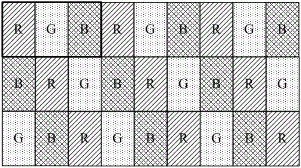
A technology of pixel structure and display panel, applied in identification devices, instruments, etc., can solve the problems of high display resolution, affect picture quality, low color saturation of display panel, etc., and achieve the effect of improving display resolution

Active Publication Date: 2015-12-23
CHONGQING BOE OPTOELECTRONICS +1
View PDF7 Cites 24 Cited by
  • Summary
  • Abstract
  • Description
  • Claims
  • Application Information

AI Technical Summary

Problems solved by technology

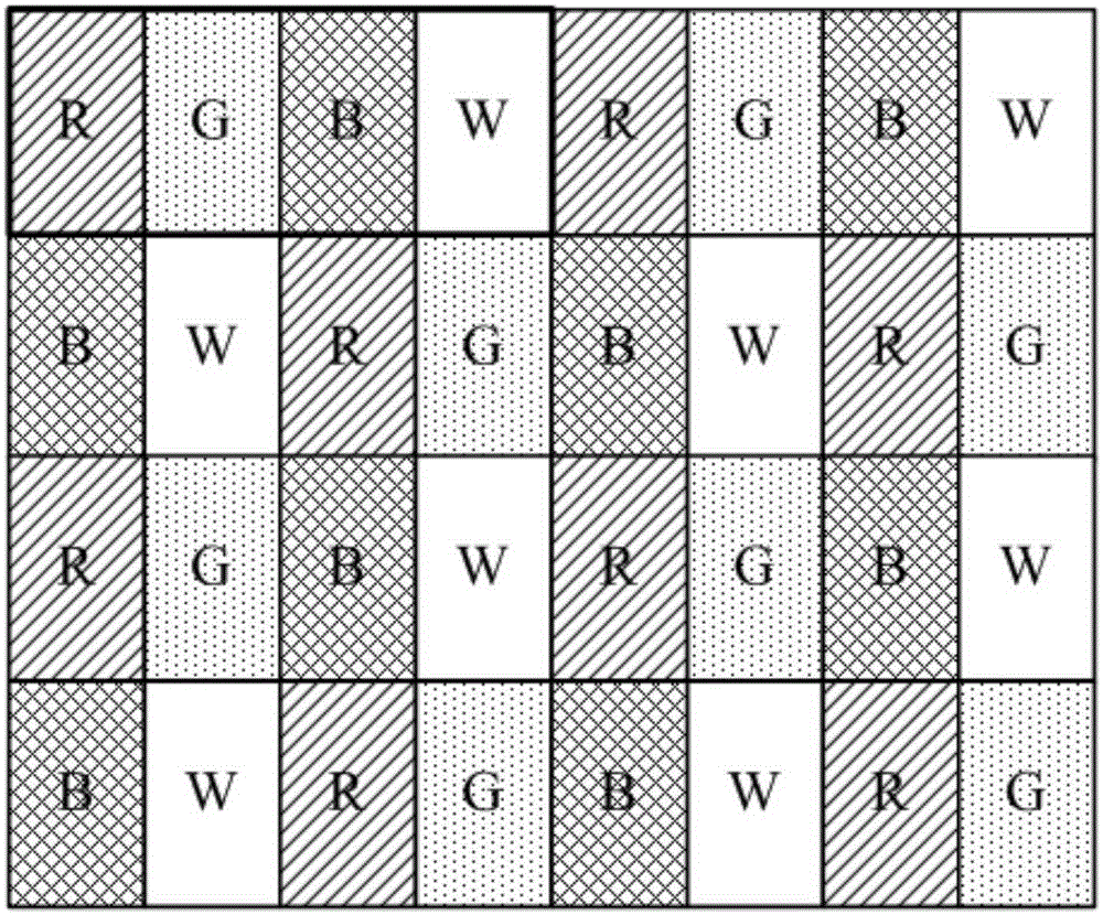
[0004] However, in the arrangement of the above-mentioned common pixel structure, when the display panel is displayed, the white sub-pixel needs to use the sub-pixels in adjacent rows or adjacent columns to completely display different colors, which will lead to the color saturation of the display panel. It will be low, which will affect the picture quality, making the picture quality rougher, and the junction between light and dark in the displayed image is too obvious. At the same time, the pixel structure including R, G, B, and W sub-pixels does not include R, G, and B sub-pixels. The actual display resolution of the pixel structure is high
Moreover, in actual production, the pixel structure including R, G, B, and W sub-pixels needs to use complex IC algorithms to make up for the problem of rough image quality

Method used


Image

  • Pixel structure, display panel and display device
  • Pixel structure, display panel and display device
  • Pixel structure, display panel and display device

Examples


Embodiment Construction

[0030] The specific implementation manners of the pixel structure, the display panel and the display device provided by the embodiments of the present invention will be described in detail below with reference to the accompanying drawings.

[0031] Wherein, the size and shape of each sub-pixel in the drawings does not reflect the real proportion of the display panel, and is only a partial structure of the display panel, for the purpose of schematically illustrating the content of the present invention.

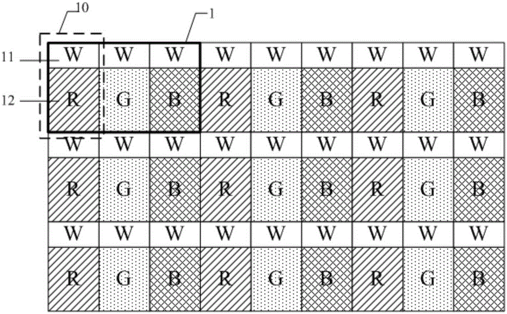
[0032] An embodiment of the present invention provides a pixel structure, such as Figure 2a and Figure 2b As shown, it includes several pixel unit groups 1 ( Figure 2a and Figure 2b The marked part of the solid line box in the middle represents a pixel unit group), the pixel unit group 1 includes three sub-pixel groups 10 arranged side by side along the row direction ( Figure 2a and Figure 2b The dotted box in the middle represents a sub-pixel group); among them,

...


PUM


Abstract

The invention discloses a pixel structure, a display panel and a display device. The pixel structure comprises multiple pixel unit groups which are arranged in an array mode, and each pixel unit group comprises three sub-pixel groups which are arranged side by side in the first direction, wherein each sub-pixel group comprises two sub pixels, namely, a white sub pixel and a monochrome sub pixel, which are arranged side by side in the second direction, and colors of the three monochrome sub pixels in the same pixel unit group are all different. According to the pixel structure, each sub-pixel group comprises one white sub pixel and one monochrome sub pixel corresponding to the white sub pixel, and compared with an existing a pixel structure comprising sub pixels with four colors, the actual display resolution can be improved, and the problem that the picture quality is rough cannot be caused.

Description

technical field [0001] The invention relates to the field of display technology, in particular to a pixel structure, a display panel and a display device. Background technique [0002] A plurality of pixels are arranged in an existing display panel, and each pixel is composed of at least three sub-pixels with different colors. When each pixel is composed of three sub-pixels with different colors, the three sub-pixels are red (R) sub-pixel, green (G) sub-pixel and blue (B) sub-pixel, when the display panel needs to display a certain color , by adjusting the grayscale values ​​of the R, G, and B sub-pixels, the color can be combined. At present, the most common arrangement of pixel structures is as follows: Figure 1a The arrangement shown ( Figure 1a A solid line box in the center indicates a pixel). [0003] At present, the light transmittance of the sub-pixels of R, G, and B colors is much lower than that of the white sub-pixel during display. Therefore, in the prior art...

Claims


Application Information

Patent Timeline
IPC IPC(8): G09F9/30
CPCG09F9/30
Inventor 汪锐李少茹金在光尚飞
Owner CHONGQING BOE OPTOELECTRONICS
Learn More