
Micro-transfer-printed light-emitting diode device
a technology of light-emitting diodes and micro-transfers, which is applied in the direction of solid-state devices, basic electric elements, electric devices, etc., can solve the problems of increased power, reduced display and battery lifetime, and difficulty in maintaining a very high resolution, so as to reduce the area needed for micro-transfer printed devices, improve device life, and improve display resolution
- Summary
- Abstract
- Description
- Claims
- Application Information
AI Technical Summary
Benefits of technology
Problems solved by technology
Method used
Image

Examples
Embodiment Construction
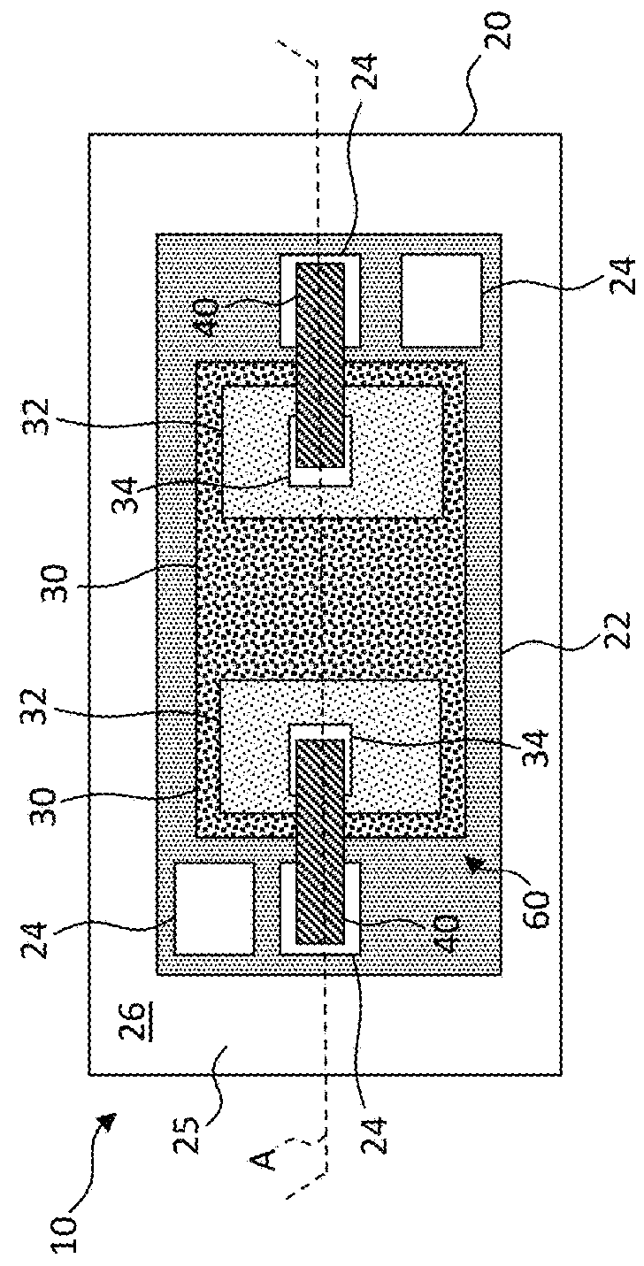
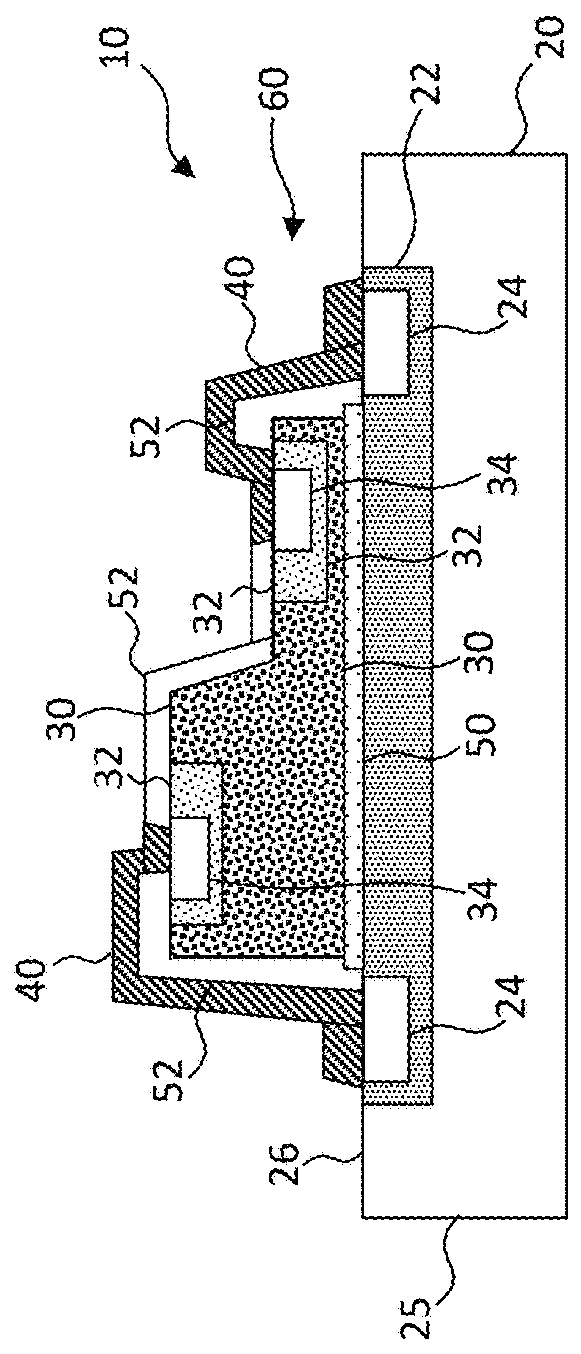
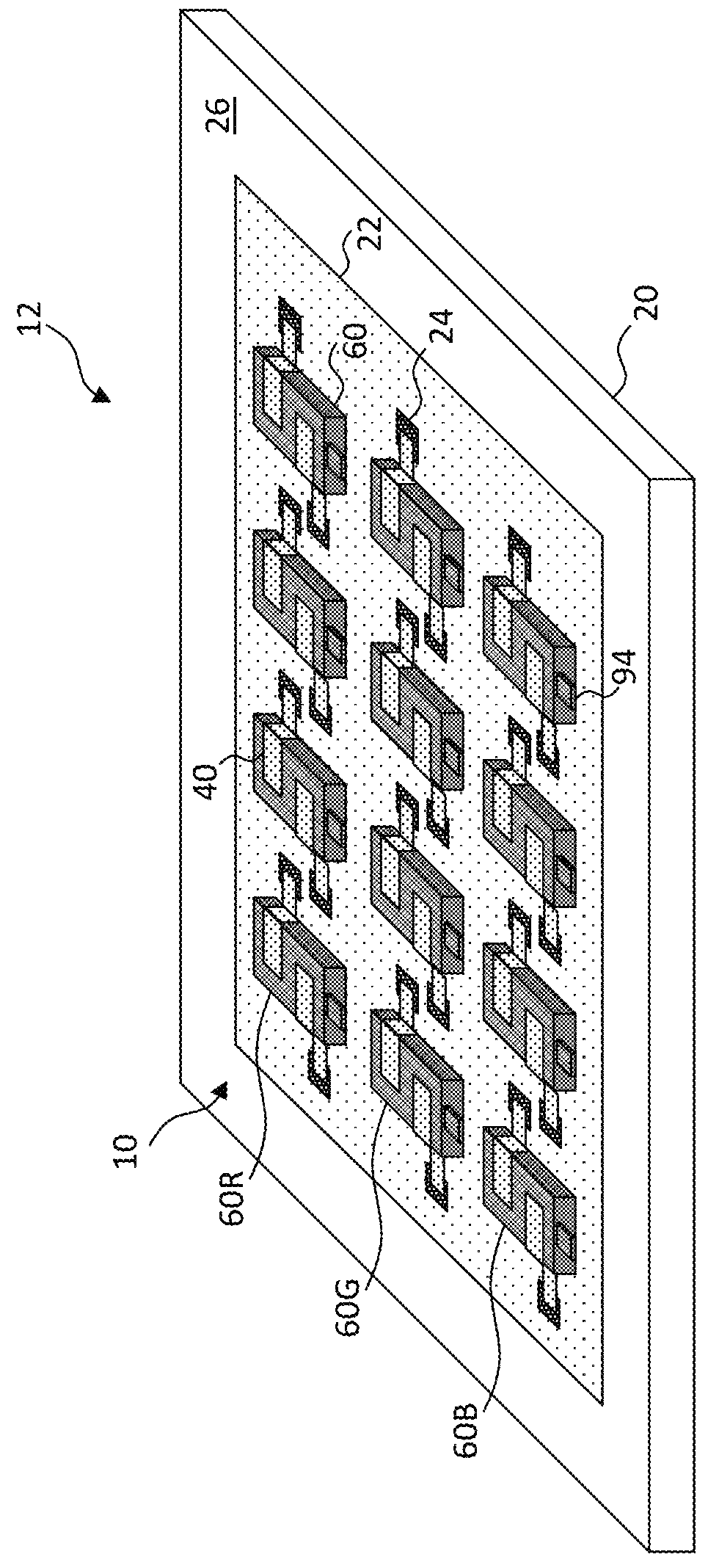
[0040]Referring to the schematic plan view of FIG. 1A, the schematic cross section of FIG. 1B taken across cross section line A of FIG. 1A, and the perspective of FIG. 2, in an embodiment of the present invention, a compound LED device 10 includes a semiconductor substrate 20. The semiconductor substrate 20 can be a silicon substrate. The semiconductor substrate 20 includes an active electronic circuit 22, for example a CMOS transistor circuit, formed in or on the semiconductor substrate 20, for example, using photolithographic methods and materials found in the integrated circuit industry. The active electronic circuit 22 can be, for example, an active-matrix circuit for driving one or more LEDs 60 in a display. The semiconductor substrate 20 or active electronic circuit 22 includes two or more electrically conductive circuit connection pads 24, formed in or on the semiconductor substrate 20, for providing control, power, or ground signals to the active electronic circuit 22 or rec...
PUM
 Abstract
Description
Claims
Application Information